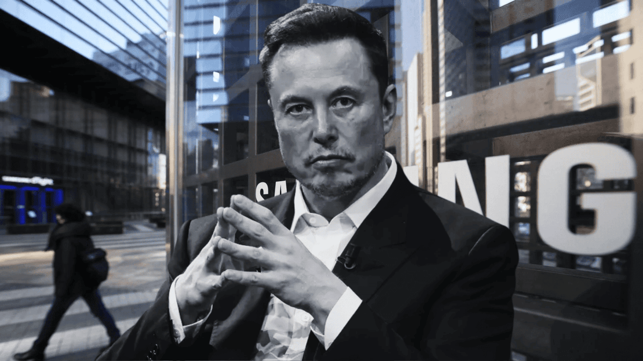
Tesla Partners with Samsung for AI5 Chip Production as Musk Claims Korean Fab Outperforms TSMC's Arizona Facility
3 Sources
3 Sources
[1]
Musk says Samsung's Texas fab outclasses TSMC's US-based fabs -- with AI5 still in development, questions remain over whether Tesla will need advanced tools
Last week, Elon Musk announced that Tesla would make its next-generation AI5 processor in the U.S. and would double-source this system-on-chip from both TSMC and Samsung Foundry. This is down to Tesla aiming to have plenty of AI5 silicon available, since it will be used in a wide range of applications, including cars, robots, and, somewhat unusually, data centers. Musk also said that Samsung Foundry's fab in Taylor, Texas, is more advanced than TSMC's Fab 21 phase 1 in Arizona, which is a strange comment from a fabless chip designer. We analyze what Samsung's Texas fab is capable of, how it compares to TSMC's fab 21 phase 1, and whether Musk's upcoming AI5 chip will really need the advanced capabilities that Samsung Foundry can offer. Tesla's AI5 will be considerably more advanced than the AI4, according to Elon Musk. Since the company plans to use them broadly across its products, the company wishes to have a surplus of supply. "I am confident [the AI5] will be winner, next level [of AI performance], so it makes sense to have both Samsung and TSMC focused on AI5," Musk said during an earnings call with investors and financial analysts this week. Based on Musk's earlier comments, AI5 is a massive processor which can demand up to 800W (at peak). Without plenty of rudimentary IPs such as image signal processing or graphics processing, it leaves die space for low-precision tensor compute hardware to maximize performance and cost efficiency. Despite the high power consumption, the AI5 fits in 'a half reticle,' which equates to around 430mm^2, putting it in a happy middleground of not being too large, nor too small. The exact configuration of Tesla's AI5 next-generation system-on-chip (assuming that it is a SoC, not a multi-chiplet SiP, or a series of products) is unknown; we only know it contains Arm CPU cores and plenty of proprietary Tesla hardware. Due to this, it's difficult to ascertain just what lies under the hood of AI5, given its vast differences from the AI4 in terms of power consumption (800W vs. 140W), lack of graphics processing and image processing capabilities and the wide range of potential applications, which span from cars and robots, to data centers. "If we have too many AI5 chips for the cars and robots, we can always put them in the data center," Musk said. "So, we already use AI4 for training in our in our data center. So, [we] use a combination of AI4 and Nvidia hardware. So, we are not about to replace Nvidia, to be clear, but we do use both in combination, AI4 and Nvidia hardware. And the AI5 excess production, can always put in our data centers." While Musk outlined vast volumes as one of the primary reasons behind the rather unusual decision of double sourcing a complex chip from two advanced foundries on two advanced nodes (which are yet to be determined), is perhaps another reason is to 'pipe clean' Samsung Foundry's American fab before assigning AI6 production exclusively (or maybe not exclusively) to SF, but Musk denied it. Musk also made an unusual comment regarding Samsung's Taylor, Texas fab tools, claiming that they are more advanced than TSMC's Fab 21 phase 1 in Arizona. "Technically, the Samsung fab [in Texas] has slightly more advanced equipment than the TSMC fab [in Arizona]. These [AI5 chips] will be made in the U.S. [...] by TSMC in Arizona, Samsung in Texas," Musk said. Samsung's fab in Taylor, Texas, has been designed to produce chips on various manufacturing technologies, down to Samsung Foundry's SF2, which used to be called SF3P, but given its performance advantages over other SF3-series nodes, the company decided to bring it into the 2nm-class league. However, whether or not SF2 is competitive compared to Intel Foundry's 18A and TSMC's N2 is something that remains to be seen, as other details, such as the number of EUV layers SF2 uses, are still a mystery. While we do not know the exact configuration of Samsung Foundry's fab in Taylor, Texas, you can presume that it is tailored to make chips on 3nm-class process technologies, given its ramp timing in 2026 - 2027. So, we can expect Samsung to equip its fab for SF2P, SF2X, SF2A, and perhaps SF2Z (with backside power delivery), but this has not been officially confirmed. Still, a fab capable of producing 3nm-class chips is indeed more advanced than TSMC's Fab 21 phase 1 in Arizona, which is designed to make chips on 5nm and 4nm-class production nodes. So, TSMC's fab 21 lags behind Samsung by design. Also, keep in mind that Samsung's leading-edge process technologies have relied on gate-all-around (GAA) transistors since SF3 in 2022, which require a specific set of tools to create them. TSMC's Fab 21 phase 1 was designed and equipped between 2020 - 2024 (it probably follows TSMC's blueprints for its 1st Generation EUV-capable fabs). This is notably before ASML released its newer Twinscan NXE:3800E lithography systems, so the fab comes equipped with the Twinscan NXE:3600D machines, which can process up to 160 wafers per hour, at a dose of 30 mJ/cm^2. In contrast, Samsung Foundry's fab in Taylor is being equipped now, so if we were to speculate, we would imagine that Samsung equipped its fab in Taylor, Texas, with the more advanced Twinscan NXE:3800E, which processes up to 220 wafers per hour at 30 mJ/cm^2. Do bear in mind that ASML's scanners are upgradeable, so theoretically, TSMC can boost the performance of the tools it uses, if it's deemed to be necessary. Because Samsung Foundry's fab in Taylor, Texas, is meant to produce chips relying on GAA transistors, it has more significant differences from TSMC's Fab 21 phase 1, which is designed to produce ICs with tried-and-true FinFET transistors. GAA transistors introduce an entirely new level of complexity in both etching and deposition, because their architecture replaces a single vertical fin with multiple stacked horizontal nanosheets. Each sheet is separated by a temporary silicon-germanium (SiGe) layer that must be selectively etched away without damaging the adjacent silicon channels. This requires atomic-layer etch (ALE) tools capable of removing material one or two angstroms at a time with extreme selectivity and directionality. These systems must also achieve near-perfect uniformity across 300mm wafers, since even slight over-etching can collapse or roughen the ultra-thin nanosheets. While TSMC hardly needs such tools at Fab 21 phase 1, Samsung needs them in its Taylor fab. On the deposition front, conformal atomic-layer deposition (ALD) and selective epitaxy are key to device performance. The gate in a GAA device wraps fully around each nanosheet, requiring metal and dielectric films that are pinhole-free and uniform on all surfaces, even deep inside narrow trenches. To produce them, chipmakers need tools that provide sub-angstrom control of high-k dielectrics (e.g., HfO₂) and metal gate layers (TiN, Ru, Mo) with near-perfect step coverage. In addition, selective epitaxial deposition systems grow alternating Si/SiGe multilayers that form the nanosheet stack with atomic-scale thickness precision. Together, these advanced etch and deposition systems provide the precision and process stability necessary to manufacture GAA transistors reliably at the 3nm node and beyond. However, GAA transistors are not required for TSMC's N4 or N5 processes. TSMC is expected to debut GAA transistors in its 1.6nm-class 16A process. Since the Samsung fab in Taylor, Texas, is at least one production node ahead of TSMC's Fab 21 phase 1, it features different metrology and inspection tools, too. Fab 21 phase 1 likely features a standard toolset from the late 2010s and early 2020s, so its in-line metrology/inspection stack is comprised of overlay/CD scatterometry, optical wafer inspection, and e-beam review tuned for 4nm and 5nm nodes. In contrast, Samsung's fab in Texas uses new generation tools, such as multi-angle scatterometry, X-ray, and e-beam or even multi e-beam metrology to ensure sub-angstrom control and uniformity across wafers. With the differences between the fabs out of the way, another question remains: Does Tesla's AI5 chip demand the advanced tools that Samsung Foundry's Taylor fab can provide? The simple answer is that we don't know, given the lack of specifics we have about AI5. The processor was expected to be released in early 2026, but then Tesla delayed it to late 2026. As Musk revealed last week, the hardware is still in development and has not taped out, so it is well over a year away from production. "The AI5 chip designed by Tesla is, I think it is an amazing design, I have spent almost every weekend for the last few months with the chip design team working on AI5," said Musk. "I do not hand out praise easily, but I have to say that I think I think the Tensor chip team is really designing an incredible chip here. This is by some metrics, the AI5 chip will be 40 times better than the AI4 chip. Not 40%, 40 times. Because we have a detailed understanding of the entire software and hardware stack." If Tesla tapes out AI5 this November, then the earliest time when it can start its mass production is December 2026. A more realistic timeframe is likely early 2027. In any case, Samsung's Taylor fab is expected to start ramping up chip production sometime in 2026, so by late 2026 or early 2027, it will be ready for AI5. As for TSMC, the 3nm-capable Fab 21 phase 2 will only ramp in the second half of 2027. So, if Tesla plans to double-source AI5 from TSMC and Samsung Foundry starting in late 2026 or early 2027, it will likely rely on TSMC's N5A in Arizona and, presumably the SF4A fabrication process in Texas. In theory, Tesla could use SF2A, but we doubt it will be ready for large processors by early 2027, so SF4A is more likely, as by that time, it will be a mature automotive-grade fabrication technology. Furthermore, making the same chip on a 5nm-class process technology and Samsung's SF2 does not make a lot of sense, as the final silicon will offer different power, thermal, and performance characteristics. Given that Tesla's AI5 will almost certainly rely on FinFET transistors, it will barely make use of the more advanced tools that Samsung will have at its fab in Taylor, Texas, making Musk's comment largely irrelevant for the AI5 processor. Perhaps, the main advantage of SF's fab for Tesla's AI5 is its Twinscan NXE:3800E lithography systems, which can process 40% more wafers per hour than their predecessors used at Fab 21 phase 1. This can potentially shrink cycle time and/or increase output. However, actual cycle time improvement across the entire fab is much smaller, as EUV exposure is only one part of a multi-hundred-step process. Other tools, such as deposition, etch, inspection and cleaning dominate total wafer cycle time, which is around 12 weeks for 5nm-class products. So at best, the newer ASML tools might cut total wafer cycle time by 5% - 10%, but their performance advantage over predecessors will not translate into a 40% lower cycle time. To sum things up, Musk's comment about Samsung Foundry's upcoming fab in Taylor, Texas, being 'more advanced' than TSMC's Fab 21 phase 1 is technically true, but it is largely irrelevant to Tesla's immediate production needs.
[2]
Not Just Taiwan Semiconductor: Elon Musk To Also Rely On Samsung For Tesla's AI Chips - Samsung Electronics Co (OTC:SSNLF), Tesla (NASDAQ:TSLA), Taiwan Semiconductor (NYSE:TSM)
Tesla, Inc. (NASDAQ:TSLA) chief Elon Musk announced that Samsung Electronics Co., Ltd. (OTC:SSNLF) will now co-produce the automaker's next-generation artificial intelligence chip, the AI5. The move signals a major win for Samsung as it vies for market share against the key contract chip manufacturer, Taiwan Semiconductor Manufacturing Co. (NYSE:TSM). Musk Revises Previous Manufacturing Plans During Tesla's third-quarter investor conference call on Wednesday, Musk explicitly corrected his own previous public statements, which had indicated that Taiwan Semiconductor would be the sole manufacturer for the AI5 chip, Bloomberg reported on Thursday. Also Read: Tesla's AI And Robotaxi Push Could Add $1 Trillion, Analyst Says Tesla designs these specialized AI chips to power its autonomous driving features and its developing line of robots, using them alongside processors from Nvidia Corporation (NASDAQ:NVDA). In July, Musk confirmed reports of a $16.5 billion deal for Samsung to manufacture Tesla's future AI6 chip. At that time, he noted that while Samsung was already producing the older AI4 chip, Taiwan Semiconductor would handle the AI5 -- a plan that has now evolved to include both manufacturing giants. While still a distant second to Taiwan Semiconductor, the South Korean firm is making substantial investments in a new production hub near Austin, Texas, where Tesla is also headquartered. AI Fuels Samsung's Profit Surge Samsung looks to report its largest quarterly profit in more than three years. The intense demand for AI hardware has significantly boosted sales of Samsung's specialized High-Bandwidth Memory (HBM) while also constraining the supply and driving up prices for its core business of conventional memory chips. CLSA Securities Korea and Counterpoint analysts attributed the success to several key factors. Samsung's HBM shipments surged dramatically. This, combined with strong demand from both AI and general-purpose servers, has pushed prices for standard DRAM and NAND chips. Looking ahead, Samsung is solidifying its market position for future growth. The company recently secured a critical win by getting its latest HBM chips approved for use in Nvidia's advanced AI systems. Price Action: TSLA stock was trading lower by 3.30% to $424.48 at last check Thursday. TSM was up 0.84%. Read Next: Is Amazon The Next Big AI Winner? One Analyst Thinks Wall Street Is Wrong Photo by Frederic Legrand - COMEO via Shutterstock SSNLFSamsung Electronics Co Ltd$42.480.34%OverviewTSLATesla Inc$424.06-3.40%TSMTaiwan Semiconductor Manufacturing Co Ltd$290.300.49%NVDANVIDIA Corp$179.90-0.21%Market News and Data brought to you by Benzinga APIs
[3]
Samsung's Fab Is More Advanced Than TSMC's," Claims Elon Musk, as Tesla Turns to the Korean Giant for Its Next-Gen AI5 & AI6 Chips
Elon Musk has said a few words of 'appreciation' for Samsung Foundry, which could go a long way for the Korean giant, as it manages to snag up orders for Tesla's latest AI chips. Tesla's Upcoming AI5 Chips Are Claimed to Bring In Massive Performance Improvements, Up to 10x the Previous-Generation One of the most significant achievements for Samsung's foundry division was securing orders for Tesla's AI6 chips, which were to utilize the firm's SF2 (2nm) process. This was seen as a massive breakthrough for the Korean giant, considering that Elon's partnership meant one of the first significant industry exposures to Samsung Foundry. However, at the recent Q3 earnings call, Tesla's CEO, Elon Musk, revealed that both Samsung and TSMC are responsible for producing the AI5 chips, and more importantly, Samsung's Taylor fab is "slightly advanced" compared to TSMC's Arizona facility. We do know that Tesla entered a deal with Samsung to have their AI6 chips produced in the US, but AI5 is a new addition, considering that they were previously produced exclusively at TSMC. This indicates that Samsung Foundry has garnered substantial interest from Elon himself, which is a significant deal for the Korean giant. Interestingly, Elon also discussed the firm's AI5 chips, claiming that they would offer an improvement of up to ten times over AI4. This would be a significant feat, considering that such an upgrade has been achieved by just a single generational change. Discussing the architectural changes within the AI5 chip, Musk notes that Tesla's design team has removed the 'legacy GPU block', likely referring to the general-purpose GPU onboard. Instead, the team has likely integrated AI tile kernels and similar elements for application-specific workloads that would suit Tesla's computing ambitions. Musk also mentions the "half a reticle" size of the AI5 chip, which implies a massive package with many more accelerator tiles and a larger on-chip SRAM footprint, bringing the expected performance improvements that the Tesla team desires. Elon Musk is so optimistic about AI5 that he actually wants an 'oversupply' of the chips, which means that Samsung's Taylor fab would need to ramp up production volumes to ensure they meet the anticipated demand. Securing Tesla as a client will defintely boost Samsung's efforts to produce in the U.S., ultimately paving the way for a more extensive adoption by customers. Follow Wccftech on Google or add us as a preferred source, to get our news coverage and reviews in your feeds.
Share
Share
Copy Link
Elon Musk announces Tesla will dual-source its next-generation AI5 chips from both Samsung and TSMC, with production taking place in the US. Musk claims Samsung's Texas fab has more advanced equipment than TSMC's Arizona facility.
Tesla Expands Chip Manufacturing Partnership
Tesla CEO Elon Musk announced during the company's third-quarter earnings call that the electric vehicle manufacturer will dual-source its next-generation AI5 processor from both Taiwan Semiconductor Manufacturing Company (TSMC) and Samsung Foundry
1
. This represents a significant strategic shift from Tesla's previous plan to have TSMC exclusively manufacture the AI5 chips2
.
Source: Wccftech
The decision to implement a dual-sourcing strategy stems from Tesla's ambitious plans for the AI5 chip, which will power a diverse range of applications including autonomous vehicles, robots, and data centers. "I am confident [the AI5] will be winner, next level [of AI performance], so it makes sense to have both Samsung and TSMC focused on AI5," Musk stated during the investor call
1
.Samsung's Texas Facility Gains Recognition
In an unusual comment from a fabless chip designer, Musk praised Samsung Foundry's fabrication facility in Taylor, Texas, claiming it possesses more advanced equipment than TSMC's Fab 21 phase 1 in Arizona. "Technically, the Samsung fab [in Texas] has slightly more advanced equipment than the TSMC fab [in Arizona]," Musk explained
1
.
Source: Benzinga
The technical basis for this claim lies in the manufacturing capabilities of each facility. Samsung's Taylor fab is designed to produce chips using 3nm-class process technologies, including the company's SF2 node, which was previously designated as SF3P but was reclassified due to its performance advantages
1
. In contrast, TSMC's Fab 21 phase 1 was designed to manufacture chips on 5nm and 4nm-class production nodes, making it less advanced by design.AI5 Chip Specifications and Performance Expectations
The AI5 processor represents a substantial advancement over Tesla's current AI4 chip, with Musk claiming performance improvements of up to ten times the previous generation
3
. The chip is designed to consume up to 800 watts at peak performance, significantly higher than the AI4's 140-watt consumption, while fitting within a "half reticle" size of approximately 430mm²1
.Tesla's design team has made significant architectural changes to the AI5, removing the legacy GPU block and focusing die space on low-precision tensor compute hardware to maximize performance and cost efficiency
1
. This specialized approach allows the chip to excel in AI-specific workloads across Tesla's expanding product ecosystem.Related Stories


Strategic Implications for Samsung Foundry
This partnership represents a major victory for Samsung Foundry as it competes against TSMC for market share in the advanced semiconductor manufacturing space. The company had previously secured a $16.5 billion deal to manufacture Tesla's future AI6 chips, and the addition of AI5 production further solidifies the relationship
2
.Samsung's financial performance has benefited significantly from AI-driven demand, with the company expected to report its largest quarterly profit in more than three years. The surge in demand for AI hardware has boosted sales of Samsung's High-Bandwidth Memory (HBM) products while constraining supply and driving up prices for conventional memory chips
2
.References
Summarized by
Navi
[1]
Related Stories
Recent Highlights
1
AI Models Lie and Deceive to Protect Other AI Models From Deletion, Study Reveals
Science and Research

2
AI chatbots validate you too much, making you less kind to others, Stanford study reveals
Science and Research
3
Judge blocks Pentagon from blacklisting Anthropic over AI safety guardrails dispute
Policy and Regulation

Recent Highlights
Today's Top Stories


Your Daily Dose of Curated AI News
Don’t drown in AI news. We cut through the noise - filtering, ranking and summarizing the most important AI news, breakthroughs and research daily. Spend less time searching for the latest in AI and get straight to action.