China builds secret EUV prototype to rival the West in AI chips, targeting 2030 production
4 Sources
4 Sources
[1]
Exclusive: How China built its 'Manhattan Project' to rival the West in AI chips
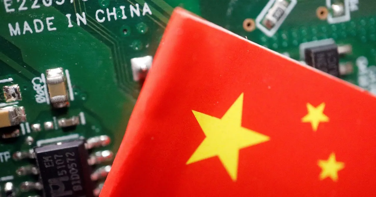
SINGAPORE Dec 17 - In a high-security Shenzhen laboratory, Chinese scientists have built what Washington has spent years trying to prevent: a prototype of a machine capable of producing the cutting-edge semiconductor chips that power artificial intelligence, smartphones and weapons central to Western military dominance, Reuters has learned. Completed in early 2025 and now undergoing testing, the prototype fills nearly an entire factory floor. It was built by a team of former engineers from Dutch semiconductor giant ASML (ASML.AS), opens new tab who reverse-engineered the company's extreme ultraviolet lithography machines or EUVs, according to two people with knowledge of the project. EUV machines sit at the heart of a technological Cold War. They use beams of extreme ultraviolet light to etch circuits thousands of times thinner than a human hair onto silicon wafers, currently a capability monopolized by the West. The smaller the circuits, the more powerful the chips. China's machine is operational and successfully generating extreme ultraviolet light, but has not yet produced working chips, the people said. In April, ASML CEO Christophe Fouquet said that China would need "many, many years" to develop such technology. But the existence of this prototype, reported by Reuters for the first time, suggests China may be years closer to achieving semiconductor independence than analysts anticipated. Nevertheless, China still faces major technical challenges, particularly in replicating the precision optical systems that Western suppliers produce. The availability of parts from older ASML machines on secondary markets has allowed China to build a domestic prototype, with the government setting a goal of producing working chips on the prototype by 2028, according to the two people. But those close to the project say a more realistic target is 2030, which is still years earlier than the decade that analysts believed it would take China to match the West on chips. Chinese authorities did not respond to requests for comment. The breakthrough marks the culmination of a six-year government initiative to achieve semiconductor self-sufficiency, one of President Xi Jinping's highest priorities. While China's semiconductor goals have been public, the Shenzhen EUV project has been conducted in secret, according to the people. The project falls under the country's semiconductor strategy, which state media has identified as being run by Xi Jinping confidant Ding Xuexiang, who heads the Communist Party's Central Science and Technology Commission. Chinese electronics giant Huawei plays a key role coordinating a web of companies and state research institutes across the country involving thousands of engineers, according to the two people and a third source. The people described it as China's version of the Manhattan Project, the U.S. wartime effort to develop the atomic bomb. "The aim is for China to eventually be able to make advanced chips on machines that are entirely China-made," one of the people said. " China wants the United States 100% kicked out of its supply chains." Huawei, the State Council of China, the Chinese Embassy in Washington, and China's Ministry of Industry and Information Technology did not respond to requests for comment. Until now, only one company has mastered EUV technology: ASML, headquartered in Veldhoven, Netherlands. Its machines, which cost around $250 million, are indispensable for manufacturing the most advanced chips designed by companies like Nvidia and AMD -- and produced by chipmakers such as TSMC, Intel, and Samsung. ASML built its first working prototype of EUV technology in 2001, and told Reuters it took nearly two decades and billions of euros in R&D spending before it produced its first commercially-available chips in 2019. "It makes sense that companies would want to replicate our technology, but doing so is no small feat," ASML told Reuters in a statement. ASML's EUV systems are currently available to U.S. allies including Taiwan, South Korea, and Japan. Starting in 2018, the United States began pressuring the Netherlands to block ASML from selling EUV systems to China. The restrictions expanded in 2022, when the Biden administration imposed sweeping export controls designed to cut off China's access to advanced semiconductor technology. The controls targeted not just EUV systems but also older deep ultraviolet (DUV) lithography machines that produce less-advanced chips like Huawei's, aiming to keep China at least a generation behind in chipmaking capabilities. The U.S. State Department said the Trump Administration has strengthened enforcement of export controls on advanced semiconductor manufacturing equipment and is working with partners "to close loopholes as technology advances." The Dutch Ministry of Defence said the Netherlands is developing policies requiring "knowledge institutions" to perform personnel screenings to prevent access to sensitive technology "by individuals that have ill intentions or who are at risk of being pressured." Export restrictions have slowed China's progress toward semiconductor self-sufficiency for years, and constrained advanced chip production at Huawei, the two people and a third person said. The sources spoke on condition they not be identified due to the confidentiality of the project. CHINA'S MANHATTAN PROJECT One veteran Chinese engineer from ASML recruited to the project was surprised to find that his generous signing bonus came with an identification card issued under a false name, according to one of the people, who was familiar with his recruitment. Once inside, he recognized other former ASML colleagues who were also working under aliases and was instructed to use their fake names at work to maintain secrecy, the person said. Another person independently confirmed that recruits were given fake IDs to conceal their identities from other workers inside the secure facility. The guidance was clear, the two people said: Classified under national security, no one outside the compound could know what they were building -- or that they were there at all. The team includes recently retired, Chinese-born former ASML engineers and scientists -- prime recruitment targets because they possess sensitive technical knowledge but face fewer professional constraints after leaving the company, the people said. Two current ASML employees of Chinese nationality in the Netherlands told Reuters they have been approached by recruiters from Huawei since at least 2020. Huawei did not respond to requests for comment. European privacy laws limit ASML's ability to track former employees. Though employees sign non-disclosure agreements, enforcing them across borders has proven difficult. ASML won an $845 million judgment in 2019 against a former Chinese engineer accused of stealing trade secrets, but the defendant filed for bankruptcy and continues to operate in Beijing with Chinese government support, according to court documents. ASML told Reuters that it "vigilantly guards" trade secrets and confidential information. "While ASML cannot control or restrict where former employees work, all employees are bound by the confidentiality clauses in their contracts," the company said, and it has "successfully pursued legal action in response to the theft of trade secrets." Reuters was unable to determine if any legal actions have been taken against former ASML employees involved in China's lithography program. The company said it safeguards EUV knowledge by ensuring only select employees can access the information even inside the company. Dutch intelligence warned in an April report that China "used extensive espionage programmes in its attempts to obtain advanced technology and knowledge from Western countries," including recruiting "Western scientists and employees of high-tech companies." The ASML veterans made the breakthrough in Shenzhen possible, the people said. Without their intimate knowledge of the technology, reverse-engineering the machines would have been nearly impossible. Their recruitment was part of an aggressive drive China launched in 2019 for semiconductor experts working abroad, offering signing bonuses that started at 3 million to 5 million yuan ($420,000 to $700,000) and home-purchase subsidies, according to a Reuters review of government policy documents. Recruits included Lin Nan, ASML's former head of light source technology, whose team at the Chinese Academy of Sciences' Shanghai Institute of Optics has filed eight patents on EUV light sources in 18 months, according to patent filings. The Shanghai Institute of Optics and Fine Mechanics did not respond to requests for comment. Lin could not be reached for comment. Two additional people familiar with China's recruitment efforts said some naturalized citizens of other countries were given Chinese passports and allowed to maintain dual citizenship. China officially prohibits dual citizenship and did not answer questions on issuing passports. Chinese authorities did not respond to requests for comment. INSIDE CHINA'S EUV FAB ASML's most advanced EUV systems are roughly the size of a school bus, and weigh 180 tons. After failed attempts to replicate its size, the prototype inside the Shenzhen lab became many times larger to improve its power, according to the two people. The Chinese prototype is crude compared to ASML's machines but operational enough for testing, the people said. China's prototype lags behind ASML's machines largely because researchers have struggled to obtain optical systems like those from Germany's Carl Zeiss AG, one of ASML's key suppliers, the two people said. Zeiss declined to comment. The machines fire lasers at molten tin 50,000 times per second, generating plasma at 200,000 degrees Celsius. The light is focused using mirrors that take months to produce, according to Zeiss' website. China's top research institutes have played key roles in developing homegrown alternatives, according to the two people. The Changchun Institute of Optics, Fine Mechanics and Physics at the Chinese Academy of Sciences (CIOMP) achieved a breakthrough in integrating extreme-ultraviolet light into the prototype's optical system, enabling it to become operational in early 2025, one of the people said, though the optics still require significant refinement. CIOMP did not respond to requests for comment. In a March online recruitment call on its website, the institute said it was offering "uncapped" salaries to PhD lithography researchers and research grants worth up to 4 million yuan ($560,000) plus 1 million yuan ($140,000) in personal subsidies. Jeff Koch, an analyst at research firm SemiAnalysis and a former ASML engineer, said China will have achieved "meaningful progress" if the "light source has enough power, is reliable, and doesn't generate too much contamination." "No doubt this is technically feasible, it's just a question of timeline," he said. "China has the advantage that commercial EUV now exists, so they aren't starting from zero." To get the required parts, China is salvaging components from older ASML machines and sourcing parts from ASML suppliers through secondhand markets, the two people said. Networks of intermediary companies are sometimes used to mask the ultimate buyer, the people said. Export-restricted components from Japan's Nikon and Canon are being used for the prototype, one of the people and an additional source said. Nikon declined to comment. Canon said it was not aware of such reports. The Japanese Embassy in Washington did not respond to a request for comment. International banks regularly auction older semiconductor fabrication equipment, the sources said. Auctions in China sold older ASML lithography equipment as recently as October 2025, according to a review of listings on Alibaba Auction, an Alibaba-owned platform. A team of around 100 recent university graduates is focused on reverse-engineering components from both EUV and DUV lithography machines, according to the people. Each worker's desk is filmed by an individual camera to document their efforts to disassemble and reassemble parts -- work the people described as key to China's lithography efforts. Staffers who successfully reassemble a component receive bonuses, the people said. HUAWEI SCIENTISTS SLEEP ON-SITE While the EUV project is run by the Chinese government, Huawei is involved in every step of the supply chain from chip design and fabrication equipment to manufacturing and final integration into products like smartphones, according to four people familiar with Huawei's operations. CEO Ren Zhengfei briefs senior Chinese leaders on progress, according to one of the people. The U.S. placed Huawei on an entity list in 2019, banning American companies from doing business with them without a license. Huawei has deployed employees to offices, fabrication plants, and research centers across the country for the effort. Employees assigned to semiconductor teams often sleep on-site and are barred from returning home during the work week, with phone access restricted for teams handling more sensitive tasks, according to the people. Inside Huawei, few employees know the scope of this work. "The teams are kept isolated from each other to protect the confidentiality of the project," one of the people said. " They don't know what the other teams work on." Reporting by Fanny Potkin in Singapore, additional reporting by Alexandra Alper in Washington, editing by Ken Li and Michael Learmonth Our Standards: The Thomson Reuters Trust Principles., opens new tab
[2]
How China built its 'Manhattan Project' to rival the West in AI chips
China has reportedly built a prototype EUV lithography machine. This development, achieved by former ASML engineers, aims to enable domestic production of advanced semiconductor chips. While currently undergoing testing, the machine has not yet produced working chips. China targets 2028 for functional chips, with 2030 considered more likely. This marks a significant step towards semiconductor independence. In a high-security Shenzhen laboratory, Chinese scientists have built what Washington has spent years trying to prevent: a prototype of a machine capable of producing the cutting-edge semiconductor chips that power artificial intelligence, smartphones and weapons central to Western military dominance, has learned. Completed in early 2025 and now undergoing testing, the prototype fills nearly an entire factory floor. It was built by a team of former engineers from Dutch semiconductor giant ASML who reverse-engineered the company's extreme ultraviolet lithography machines or EUVs, according to two people with knowledge of the project. EUV machines sit at the heart of a technological Cold War. They use beams of extreme ultraviolet light to etch circuits thousands of times thinner than a human hair onto silicon wafers, currently a capability monopolized by the West. The smaller the circuits, the more powerful the chips. China's machine is operational and successfully generating extreme ultraviolet light, but has not yet produced working chips, the people said. In April, ASML CEO Christophe Fouquet said that China would need "many, many years" to develop such technology. But the existence of this prototype, reported by Reuters for the first time, suggests China may be years closer to achieving semiconductor independence than analysts anticipated. Nevertheless, China still faces major technical challenges, particularly in replicating the precision optical systems that Western suppliers produce. The availability of parts from older ASML machines on secondary markets has allowed China to build a domestic prototype, with the government setting a goal of producing working chips on the prototype by 2028, according to the two people. But those close to the project say a more realistic target is 2030, which is still years earlier than the decade that analysts believed it would take China to match the West on chips. Chinese authorities did not respond to requests for comment. The breakthrough marks the culmination of a six-year government initiative to achieve semiconductor self-sufficiency, one of President Xi Jinping's highest priorities. While China's semiconductor goals have been public, the Shenzhen EUV project has been conducted in secret, according to the people. The project falls under the country's semiconductor strategy, which state media has identified as being run by Xi Jinping confidant Ding Xuexiang, who heads the Communist Party's Central Science and Technology Commission. Chinese electronics giant Huawei plays a key role coordinating a web of companies and state research institutes across the country involving thousands of engineers, according to the two people and a third source. The people described it as China's version of the Manhattan Project, the U.S. wartime effort to develop the atomic bomb. "The aim is for China to eventually be able to make advanced chips on machines that are entirely China-made," one of the people said. China wants the United States 100% kicked out of its supply chains." Huawei, the State Council of China, the Chinese Embassy in Washington, and China's Ministry of Industry and Information Technology did not respond to requests for comment. Until now, only one company has mastered EUV technology: ASML, headquartered in Veldhoven, Netherlands. Its machines, which cost around $250 million, are indispensable for manufacturing the most advanced chips designed by companies like Nvidia and AMD-and produced by chipmakers such as TSMC, Intel, and Samsung. ASML built its first working prototype of EUV technology in 2001, and told Reuters it took nearly two decades and billions of euros in R&D spending before it produced its first commercially-available chips in 2019. "It makes sense that companies would want to replicate our technology, but doing so is no small feat," ASML told Reuters in a statement. ASML's EUV systems are currently available to U.S. allies including Taiwan, South Korea, and Japan. Starting in 2018, the United States began pressuring the Netherlands to block ASML from selling EUV systems to China. The restrictions expanded in 2022, when the Biden administration imposed sweeping export controls designed to cut off China's access to advanced semiconductor technology.No EUV system has ever been sold to a customer in China, ASML told Reuters. The controls targeted not just EUV systems but also older deep ultraviolet (DUV) lithography machines that produce less-advanced chips like Huawei's, aiming to keep China at least a generation behind in chipmaking capabilities. The U.S. State Department said the Trump Administration has strengthened enforcement of export controls on advanced semiconductor manufacturing equipment and is working with partners "to close loopholes as technology advances." The Dutch Ministry of Defence said the Netherlands is developing policies requiring "knowledge institutions" to perform personnel screenings to prevent access to sensitive technology "by individuals that have ill intentions or who are at risk of being pressured." Export restrictions have slowed China's progress toward semiconductor self-sufficiency for years, and constrained advanced chip production at Huawei, the two people and a third person said. The sources spoke on condition they not be identified due to the confidentiality of the project.One veteran Chinese engineer from ASML recruited to the project was surprised to find that his generous signing bonus came with an identification card issued under a false name, according to one of the people, who was familiar with his recruitment. Once inside, he recognized other former ASML colleagues who were also working under aliases and was instructed to use their fake names at work to maintain secrecy, the person said. Another person independently confirmed that recruits were given fake IDs to conceal their identities from other workers inside the secure facility. The guidance was clear, the two people said: Classified under national security, no one outside the compound could know what they were building-or that they were there at all. The team includes recently retired, Chinese-born former ASML engineers and scientists-prime recruitment targets because they possess sensitive technical knowledge but face fewer professional constraints after leaving the company, the people said. Two current ASML employees of Chinese nationality in the Netherlands told Reuters they have been approached by recruiters from Huawei since at least 2020. Huawei did not respond to requests for comment. European privacy laws limit ASML's ability to track former employees. Though employees sign non-disclosure agreements, enforcing them across borders has proven difficult. ASML won an $845 million judgment in 2019 against a former Chinese engineer accused of stealing trade secrets, but the defendant filed for bankruptcy and continues to operate in Beijing with Chinese government support, according to court documents. ASML told Reuters that it "vigilantly guards" trade secrets and confidential information. "While ASML cannot control or restrict where former employees work, all employees are bound by the confidentiality clauses in their contracts," the company said, and it has "successfully pursued legal action in response to the theft of trade secrets." Reuters was unable to determine if any legal actions have been taken against former ASML employees involved in China's lithography program. The company said it safeguards EUV knowledge by ensuring only select employees can access the information even inside the company. Dutch intelligence warned in an April report that China "used extensive espionage programmes in its attempts to obtain advanced technology and knowledge from Western countries," including recruiting "Western scientists and employees of high-tech companies." The ASML veterans made the breakthrough in Shenzhen possible, the people said. Without their intimate knowledge of the technology, reverse-engineering the machines would have been nearly impossible. Their recruitment was part of an aggressive drive China launched in 2019 for semiconductor experts working abroad, offering signing bonuses that started at 3 million to 5 million yuan ($420,000 to $700,000) and home-purchase subsidies, according to a Reuters review of government policy documents. Recruits included Lin Nan, ASML's former head of light source technology, whose team at the Chinese Academy of Sciences' Shanghai Institute of Optics has filed eight patents on EUV light sources in 18 months, according to patent filings. The Shanghai Institute of Optics and Fine Mechanics did not respond to requests for comment. Lin could not be reached for comment. Two additional people familiar with China's recruitment efforts said some naturalized citizens of other countries were given Chinese passports and allowed to maintain dual citizenship. China officially prohibits dual citizenship and did not answer questions on issuing passports. Chinese authorities did not respond to requests for comment.ASML's most advanced EUV systems are roughly the size of a school bus, and weigh 180 tons. After failed attempts to replicate its size, the prototype inside the Shenzhen lab became many times larger to improve its power, according to the two people. The Chinese prototype is crude compared to ASML's machines but operational enough for testing, the people said. China's prototype lags behind ASML's machines largely because researchers have struggled to obtain optical systems like those from Germany's Carl Zeiss AG, one of ASML's key suppliers, the two people said. Zeiss declined to comment. The machines fire lasers at molten tin 50,000 times per second, generating plasma at 200,000 degrees Celsius. The light is focused using mirrors that take months to produce, according to Zeiss' website. China's top research institutes have played key roles in developing homegrown alternatives, according to the two people. The Changchun Institute of Optics, Fine Mechanics and Physics at the Chinese Academy of Sciences (CIOMP) achieved a breakthrough in integrating extreme-ultraviolet light into the prototype's optical system, enabling it to become operational in early 2025, one of the people said, though the optics still require significant refinement. CIOMP did not respond to requests for comment. In a March online recruitment call on its website, the institute said it was offering "uncapped" salaries to PhD lithography researchers and research grants worth up to 4 million yuan ($560,000) plus 1 million yuan ($140,000) in personal subsidies. Jeff Koch, an analyst at research firm SemiAnalysis and a former ASML engineer, said China will have achieved "meaningful progress" if the "light source has enough power, is reliable, and doesn't generate too much contamination." "No doubt this is technically feasible, it's just a question of timeline," he said. "China has the advantage that commercial EUV now exists, so they aren't starting from zero." To get the required parts, China is salvaging components from older ASML machines and sourcing parts from ASML suppliers through secondhand markets, the two people said. Networks of intermediary companies are sometimes used to mask the ultimate buyer, the people said. Export-restricted components from Japan's Nikon and Canon are being used for the prototype, one of the people and an additional source said. Nikon declined to comment. Canon said it was not aware of such reports. The Japanese Embassy in Washington did not respond to a request for comment. International banks regularly auction older semiconductor fabrication equipment, the sources said. Auctions in China sold older ASML lithography equipment as recently as October 2025, according to a review of listings on Alibaba Auction, an Alibaba-owned platform. A team of around 100 recent university graduates is focused on reverse-engineering components from both EUV and DUV lithography machines, according to the people. Each worker's desk is filmed by an individual camera to document their efforts to disassemble and reassemble parts-work the people described as key to China's lithography efforts. Staffers who successfully reassemble a component receive bonuses, the people said.While the EUV project is run by the Chinese government, Huawei is involved in every step of the supply chain from chip design and fabrication equipment to manufacturing and final integration into products like smartphones, according to four people familiar with Huawei's operations. CEO Ren Zhengfei briefs senior Chinese leaders on progress, according to one of the people. The U.S. placed Huawei on an entity list in 2019, banning American companies from doing business with them without a license. Huawei has deployed employees to offices, fabrication plants, and research centers across the country for the effort. Employees assigned to semiconductor teams often sleep on-site and are barred from returning home during the work week, with phone access restricted for teams handling more sensitive tasks, according to the people. Inside Huawei, few employees know the scope of this work. "The teams are kept isolated from each other to protect the confidentiality of the project," one of the people said. " They don't know what the other teams work on."
[3]
Inside China's "Impossible" AI Breakthrough & What It Means for Global AI Power
What if one of the most tightly guarded technological monopolies in the world was suddenly challenged? In a recent video, AI Grid breaks down China's reported progress in developing a prototype for EUV lithography, a feat long considered out of reach due to its extreme complexity and the dominance of Dutch company ASML. This breakthrough, if fully realized, could disrupt the global semiconductor industry and redefine the balance of power in artificial intelligence development. With the U.S. and its allies relying on export controls to maintain their edge, China's advancements raise urgent questions about whether these restrictions have inadvertently fueled innovation rather than containment. The stakes are enormous, and the implications ripple far beyond technology into geopolitics and global security. In this overview, we'll explore the profound significance of EUV lithography and why it's the linchpin of innovative AI systems. You'll discover how China's efforts to achieve semiconductor independence could accelerate its dominance in AI research, potentially reshaping the global technological landscape. But this isn't just a story of innovation, it's also a cautionary tale about the risks of an unchecked AI race and the fragility of existing power structures. Whether you're fascinated by the science behind EUV technology or concerned about its geopolitical ramifications, this breakdown will leave you questioning how prepared the world is for such a seismic shift. China's EUV Breakthrough What is EUV Lithography and Why Does It Matter? EUV lithography is a cornerstone of modern semiconductor manufacturing, allowing the production of chips with nanometer-scale precision. These chips are essential for powering AI systems, from machine learning algorithms to specialized AI processors. Key features of EUV lithography include: * Use of light with a wavelength of 13.5 nanometers, allowing intricate and compact chip designs. * Highly specialized optical systems requiring extreme precision and engineering expertise. * Exclusive production by ASML, making it a strategic asset in the global technology ecosystem. The strategic importance of EUV technology has led to strict export controls, particularly targeting China. These restrictions aim to limit China's ability to produce innovative chips, thereby slowing its technological progress and maintaining Western dominance in advanced technologies. China's Progress in EUV Technology Chinese researchers have reportedly developed a prototype EUV lithography machine capable of generating the required wavelength of light. While this prototype has not yet produced functional chips, its operational status represents a critical milestone in China's technological journey. This progress has been achieved through: * Using expertise from former ASML engineers who contributed essential knowledge. * Reverse engineering of key components to replicate the technology's functionality. * Overcoming technical barriers, though challenges remain in refining precision optics and achieving commercial scalability. Although still in its early stages, this development underscores China's determination to close the technological gap and establish itself as a leader in semiconductor innovation. China's "Impossible" AI Breakthrough Explained Advance your skills in EUV Lithography by reading more of our detailed content. Strategic Implications for Semiconductor Independence If China successfully commercializes EUV lithography, it could fundamentally alter the global semiconductor industry. Achieving self-sufficiency in chip manufacturing would allow China to: * Reduce its reliance on Western technology and supply chains, enhancing its technological sovereignty. * Domestically produce advanced AI chips, accelerating its AI development and innovation capabilities. * Neutralize the impact of export controls designed to limit its technological progress. Experts project that China could achieve commercial chip production using EUV technology by 2028-2030, significantly ahead of earlier estimates. This accelerated timeline highlights the urgency for Western nations to reassess their strategies and maintain their competitive edge in the semiconductor sector. Geopolitical and Economic Ramifications The potential success of China's EUV technology has profound geopolitical and economic implications. The U.S. and its allies have long relied on their technological superiority to maintain leadership in military, economic, and AI capabilities. A shift in this balance could: * Weaken the West's influence in global technology and innovation ecosystems. * Accelerate China's rise as a dominant player in AI and other advanced fields, reshaping global power dynamics. * Expose the limitations of export controls, which may have inadvertently driven China to innovate independently. This development also raises critical questions about the effectiveness of current policies in a rapidly evolving technological landscape. As China progresses, Western nations may need to explore alternative strategies to maintain their competitive edge while fostering global stability. Implications for the Global AI Race China's advancements in semiconductor technology could significantly influence the global AI race. With access to advanced AI chips, China could: * Accelerate its AI research and development, potentially surpassing Western efforts in key areas. * Shorten the timeline for achieving artificial general intelligence (AGI), a fantastic milestone in AI evolution. * Prioritize rapid progress, potentially overlooking safety and ethical considerations in the process. Unlike the U.S., where public discourse and regulatory frameworks are emerging, China's AI development process is less transparent. This lack of transparency raises concerns about governance, accountability, and the potential risks of unchecked advancements in AI technologies. China's Broader Push for Technological Sovereignty China's efforts in EUV lithography are part of a broader strategy to achieve technological independence across critical sectors. This initiative extends to areas such as: * AI model development and deployment, making sure control over foundational technologies. * Satellite navigation systems and space technology, reducing reliance on foreign infrastructure. * Advanced telecommunications and quantum computing, positioning itself as a leader in next-generation technologies. By reducing its dependence on Western innovation, China aims to insulate itself from geopolitical pressures and establish self-sufficiency in key industries. This strategy not only strengthens its domestic capabilities but also diminishes the use of Western nations in international negotiations and economic partnerships. The Risks of a Global AI Arms Race The rapid pace of technological advancement brings inherent risks, particularly in the context of a global AI race driven by competition rather than collaboration. Such a race could: * Prioritize speed over safety, increasing the likelihood of unintended consequences and technological failures. * Exacerbate geopolitical tensions, as nations compete for dominance in AI capabilities and applications. * Undermine efforts to establish international governance frameworks for AI safety and ethical standards. Without global cooperation, the potential for misuse or unchecked advancements in AI grows, emphasizing the need for robust international standards and safeguards. Collaborative efforts will be essential to mitigate risks and ensure that AI technologies are developed responsibly and equitably. Shaping the Future of Global Technology China's reported breakthrough in EUV lithography represents a pivotal moment in the global technological landscape. By advancing toward semiconductor independence, China challenges the existing balance of power and accelerates the global AI race. This development highlights the urgency of addressing gaps in AI safety governance and fostering international collaboration. As nations navigate this shifting dynamic, the stakes for technological leadership, ethical responsibility, and global stability have never been higher.
[4]
How China built its 'Manhattan Project' to rival the West in AI chips
In a high-security Shenzhen laboratory, Chinese scientists have built what Washington has spent years trying to prevent: a prototype of a machine capable of producing the cutting-edge semiconductor chips that power artificial intelligence, smartphones and weapons central to Western military dominance. Completed in early 2025 and now undergoing testing, the prototype fills nearly an entire factory floor. It was built by a team of former engineers from Dutch semiconductor giant ASML who reverse-engineered the company's extreme ultraviolet lithography machines (EUVs), according to two people with knowledge of the project. EUV machines sit at the heart of a technological Cold War. They use beams of extreme ultraviolet light to etch circuits thousands of times thinner than a human hair onto silicon wafers, currently a capability monopolized by the West. The smaller the circuits, the more powerful the chips.
Share
Share
Copy Link
Chinese scientists have completed a prototype EUV lithography machine in a high-security Shenzhen laboratory, built by former ASML engineers through reverse engineering. The machine generates extreme ultraviolet light but hasn't produced working chips yet. China targets 2028 for functional chip production, though 2030 is more realistic—years ahead of Western estimates.
China Completes Secret EUV Lithography Prototype for AI Chips
In a high-security Shenzhen laboratory, Chinese scientists have achieved what Western export controls spent years trying to prevent: a working prototype machine capable of producing advanced semiconductor chips that power artificial intelligence, smartphones, and military systems
1
. Completed in early 2025 and now undergoing testing, the prototype machine fills nearly an entire factory floor and represents China's most significant step toward semiconductor self-sufficiency2
.
Source: Reuters
The machine was built by a team of former engineers from Dutch semiconductor giant ASML who reverse-engineered the company's extreme ultraviolet lithography machines, according to two people with knowledge of the project . EUV lithography sits at the heart of a technological Cold War, using beams of extreme ultraviolet light with a wavelength of 13.5 nanometers to etch circuits thousands of times thinner than a human hair onto silicon wafers
3
4
. The smaller the circuits, the more powerful the chips—a capability currently monopolized by the West.From Manhattan Project to Semiconductor Independence
The breakthrough marks the culmination of a six-year government initiative described by sources as China's version of the Manhattan Project, the U.S. wartime effort to develop the atomic bomb . While China's semiconductor goals have been public, the Shenzhen EUV project has been conducted in secret under President Xi Jinping's semiconductor strategy, run by his confidant Ding Xuexiang, who heads the Communist Party's Central Science and Technology Commission
2
.
Source: Geeky Gadgets
Chinese electronics giant Huawei plays a key role coordinating a web of companies and state research institutes across the country involving thousands of engineers . "The aim is for China to eventually be able to make advanced chips on machines that are entirely China-made," one source told Reuters. "China wants the United States 100% kicked out of its supply chain"
2
.
Source: Japan Times
Technical Progress and Remaining Challenges in Chip Production
China's machine is operational and successfully generating extreme ultraviolet light, but has not yet produced working chips, according to sources familiar with the project . The Chinese government has set a goal of producing working chips on the prototype by 2028, though those close to the project say a more realistic target is 2030
2
. This timeline is still years earlier than the decade analysts believed it would take China to rival the West in AI chips.China still faces major technical challenges, particularly in replicating the precision optics that Western suppliers produce . The availability of parts from older ASML machines on secondary markets has allowed China to build a domestic prototype, demonstrating how Western export restrictions may have inadvertently driven China to innovate independently
3
.Related Stories

ASML Monopoly and Western Export Controls Face Test
Until now, only one company has mastered EUV technology: ASML, headquartered in Veldhoven, Netherlands. Its machines, which cost around $250 million, are indispensable for manufacturing the most advanced chips designed by companies like Nvidia and AMD and produced by chipmakers such as TSMC, Intel, and Samsung . ASML built its first working prototype of EUV technology in 2001, and it took nearly two decades and billions of euros in R&D spending before it produced its first commercially-available chips in 2019
2
.In April, ASML CEO Christophe Fouquet said that China would need "many, many years" to develop such technology . But the existence of this prototype suggests China may be years closer to achieving semiconductor independence than analysts anticipated. Starting in 2018, the United States began pressuring the Netherlands to block ASML from selling EUV systems to China, with restrictions expanding in 2022 when the Biden administration imposed sweeping export controls designed to cut off China's access to advanced semiconductor technology .
Geopolitical Implications for Global AI Power and Technological Sovereignty
If China successfully commercializes EUV lithography, it could fundamentally alter the global semiconductor industry and shift the balance of Global AI Power
3
. Achieving technological sovereignty in chip manufacturing would allow China to reduce its reliance on Western technology and supply chains, domestically produce advanced AI chips, and accelerate its artificial intelligence development capabilities3
. The U.S. and its allies have long relied on their technological superiority to maintain leadership in military, economic, and AI capabilities. A shift in this balance could weaken the West's influence in global technology ecosystems and expose the limitations of current export restrictions, which may have inadvertently fueled innovation rather than containment3
.The accelerated timeline—potentially achieving commercial chip production by 2028-2030—highlights the urgency for Western nations to reassess their strategies in maintaining their competitive edge in the semiconductor sector
3
. This development raises critical questions about whether existing policies can effectively manage a rapidly evolving technological landscape where determined nations find alternative paths to innovation despite restrictions.References
Summarized by
Navi
Related Stories
China's Semiconductor Ambitions: Progress and Challenges in Advanced Chip Manufacturing
16 Sept 2024

China's AI Chip Challenge: Racing to Match Nvidia's Dominance
30 Sept 2025•Technology
Mistral CEO calls China's AI lag a 'fairy tale' as debate intensifies over US-China AI race
23 Jan 2026•Policy and Regulation

Recent Highlights
1
Meta unveils Muse Spark AI model as Superintelligence Labs makes its debut
Technology

2
Anthropic restricts Mythos AI model release, citing unprecedented cybersecurity capabilities
Technology

3
Anthropic sends Claude AI to psychiatrist, discovers functional emotions that shape behavior
Science and Research

Recent Highlights
Today's Top Stories


Your Daily Dose of Curated AI News
Don’t drown in AI news. We cut through the noise - filtering, ranking and summarizing the most important AI news, breakthroughs and research daily. Spend less time searching for the latest in AI and get straight to action.