Nvidia Unveils Groundbreaking Silicon Photonics Technology for Next-Gen AI Data Centers
3 Sources
3 Sources
[1]
Nvidia outlines plans for using light for communication between AI GPUs by 2026 -- silicon photonics and co-packaged optics may become mandatory for next-gen AI data centers
The extreme demands of passing communication between ever-growing clusters of AI GPUs is fueling a move towards using light for communication across the networking layers. Earlier this year, Nvidia outlined that its next-generation rack-scale AI platforms will use silicon photonics interconnects with co-packaged optics (CPO) for higher transfer rates at lower power. At the Hot Chips conference this year, Nvidia released some additional information about its next-generation Quantum-X and Spectrum-X photonics interconnection solutions and when they will arrive in 2026. Nvidia's roadmap will likely closely follow TSMC's COUPE roadmap, which unfolds in three stages. The first generation is an optical engine for OSFP connectors, offering 1.6 Tb/s data transfer while reducing power consumption. The second generation moves into CoWoS packaging with co-packaged optics, enabling 6.4 Tb/s at the motherboard level. The third generation aims for 12.8 Tb/s within processor packages and targets further cuts in power and latency. In large-scale AI clusters, thousands of GPUs must behave as one system, which introduces challenges in how these processors must be interconnected: instead of each rack having its own Tier-1 (Top-of-Rack) switch linked by short copper cables, the switches are moved to the end of the row to create a consistent, low-latency fabric across multiple racks. This relocation greatly extends the distance between servers and their first switch, which makes copper impractical at speeds like 800 Gb/s, so optical connections are required for nearly every server-to-switch and switch-to-switch link. Using pluggable optical modules in this environment introduces clear limits: data signals in such designs leave the ASIC, travel across the board and connectors, and only then are converted to light. That method produces severe electrical loss, up to roughly 22 decibels on 200 Gb/s channels, which requires compensation that uses complex processing and increases per-port power consumption to 30W (which in turn calls for additional cooling and creates a point of potential failure), which becomes almost unbearable as the scale of AI deployments grow, according to Nvidia. CPO sidesteps penalties of traditional pluggable optical modules by embedding the optical conversion engine alongside the switch ASIC, so instead of traveling over long electrical traces, the signal is coupled to fiber almost immediately. As a result, electrical loss is cut to 4 decibels, and per-port power consumption is reduced to 9W. Such a layout removes numerous components that could fail and greatly simplifies the implementation of optical interconnects. Nvidia claims that by moving away from traditional pluggable transceivers and integrating optical engines directly into switch silicon (courtesy of TSMC's COUPE platform), it achieves very substantial gains in efficiency, reliability, and scalability. Improvements of CPOs compared to pluggable modules are dramatic, according to Nvidia: a 3.5-times increase in power efficiency, a 64 times better signal integrity, 10 times boost in resiliency due to fewer active devices, and roughly 30% faster deployment because service and assembly are simpler. Nvidia will introduce CPO-based optical interconnection platforms both for Ethernet and InfiniBand technologies. First, the company plans to introduce Quantum-X InfiniBand switches in early 2026. Each switch will deliver 115 Tb/s of throughput, supporting 144 ports operating at 800 Gb/s each. The system also integrates an ASIC featuring 14.4 TFLOPS of in-network processing and supporting Nvidia's 4th Generation Scalable Hierarchical Aggregation Reduction Protocol (SHARP) to cut latency for collective operations. The switches will be liquid-cooled. In parallel, Nvidia is set to bring CPO into Ethernet with its Spectrum-X Photonics platform in the second half of 2026. This one will rely on the Spectrum-6 ASIC that will power two devices: the SN6810 that provides 102.4 Tb/s of bandwidth with 128 ports at 800 Gb/s, and the larger SN6800 that scales to 409.6 Tb/s and 512 ports at the same rate. Both also use liquid cooling. Nvidia envisions that its CPO-based switches will power new AI clusters for generative AI applications that are getting larger and more sophisticated. Due to the usage of CPO, such clusters will eliminate thousands of discrete components, offering faster installation, easier servicing, and reduced power consumption per connection. As a result, clusters using Quantum-X InfiniBand and Spectrum-X Photonics offer improvements when it comes to such metrics as time-to-turn-on, time-to-first-token, and long-term reliability. Nvidia stresses that co-packaged optics are not an optional enhancement but a structural requirement for future AI data centers, which implies that the company will position its optical interconnects as some of the key advantages over rack-scale AI solutions from rivals, such as AMD. Which is, of course, why AMD has acquired Enosemi. One important thing to note about Nvidia's silicon photonics initiative is that its evolution is tightly aligned with the evolution of TSMC's COUPE (Compact Universal Photonic Engine) platform, which is set to evolve in the coming years, thus improving Nvidia's CPO platforms too. TSMC's 1st Gen COUPE is built by stacking a 65nm electronic integrated circuit (EIC) with a photonic integrated circuit (PIC) using the company's SoIC-X packaging technology. TSMC's COUPE roadmap unfolds in three stages. The first generation is an optical engine for OSFP connectors, offering 1.6 Tb/s data transfer while reducing power consumption. The second generation moves into CoWoS packaging with co-packaged optics, enabling 6.4 Tb/s at the motherboard level. The third generation aims for 12.8 Tb/s within processor packages and targets further cuts in power and latency.
[2]
Nvidia to deploy light based GPU interconnects by 2026
The company's Quantum X InfiniBand and Spectrum X Ethernet platforms will deliver up to 409.6 Tbps using liquid cooled switches built on TSMC COUPE tech. Nvidia is planning to implement light-based communication between its artificial intelligence GPUs by 2026, utilizing silicon photonics interconnects with co-packaged optics (CPO) in its next-generation rack-scale AI platforms to achieve higher transfer rates at reduced power consumption. At the Hot Chips conference, Nvidia provided further details regarding its upcoming Quantum-X and Spectrum-X photonics interconnection solutions, outlining their expected arrival in 2026. These solutions represent a significant move towards optical interconnects to manage the increasing demands of data transfer within large AI GPU clusters. Nvidia's developmental timeline is expected to closely mirror TSMC's COUPE (Compact Universal Photonic Engine) roadmap, which is structured into three distinct phases. The initial phase involves an optical engine designed for OSFP connectors, facilitating data transfers of 1.6 Tb/s while simultaneously lowering power consumption. The second phase transitions to CoWoS packaging incorporating co-packaged optics, thereby achieving 6.4 Tb/s data transfer rates at the motherboard level. The third phase focuses on achieving 12.8 Tb/s within processor packages, with the objective of further decreasing both power usage and latency. The necessity for CPO stems from the challenges associated with interconnecting thousands of GPUs in large-scale AI clusters, requiring them to operate as a unified system. This architecture necessitates modifications to traditional networking configurations. Specifically, instead of each rack having its own Tier-1 (Top-of-Rack) switch connected by short copper cables, the switches are relocated to the end of the row. This configuration establishes a consistent, low-latency fabric spanning multiple racks. This relocation increases the distance between servers and their primary switch, rendering copper cables impractical for high speeds such as 800 Gb/s. Consequently, optical connections become essential for nearly all server-to-switch and switch-to-switch links. Nvidia designs slower B30A chip to meet US restrictions The use of pluggable optical modules in such environments presents inherent limitations. In these designs, data signals exit the Application-Specific Integrated Circuit (ASIC), traverse the board and connectors, and are subsequently converted to light. This process introduces significant electrical loss, reaching approximately 22 decibels on 200 Gb/s channels. Compensation for this loss requires complex processing, which increases per-port power consumption to 30W. This, in turn, necessitates additional cooling and introduces potential points of failure. Nvidia asserts that these issues become increasingly problematic as the scale of AI deployments expands. CPO mitigates the drawbacks associated with traditional pluggable optical modules by integrating the optical conversion engine directly alongside the switch ASIC. This proximity allows the signal to be coupled to fiber almost immediately, bypassing the need to travel over extended electrical traces. As a result, electrical loss is reduced to 4 decibels, and per-port power consumption decreases to 9W. This arrangement also eliminates numerous components that could potentially fail, simplifying the implementation of optical interconnects. Nvidia asserts that transitioning from conventional pluggable transceivers and integrating optical engines directly into switch silicon, facilitated by TSMC's COUPE platform, yields substantial improvements in efficiency, reliability, and scalability. Nvidia reports that CPO offers significant advantages over pluggable modules, including a 3.5-times increase in power efficiency, a 64 times improvement in signal integrity, a 10 times increase in resilience due to the reduction in active devices, and approximately 30% faster deployment times due to simpler service and assembly procedures. Nvidia plans to introduce CPO-based optical interconnection platforms for both Ethernet and InfiniBand technologies. The company anticipates launching Quantum-X InfiniBand switches in early 2026. Each switch is designed to provide 115 Tb/s of throughput, accommodating 144 ports operating at 800 Gb/s each. The system also incorporates an ASIC featuring 14.4 TFLOPS of in-network processing and supports Nvidia's 4th Generation Scalable Hierarchical Aggregation Reduction Protocol (SHARP), aimed at reducing latency for collective operations. These switches will utilize liquid cooling. Concurrently, Nvidia is preparing to integrate CPO into Ethernet through its Spectrum-X Photonics platform, scheduled for release in the second half of 2026. This platform will be based on the Spectrum-6 ASIC, which will power two distinct devices: the SN6810, offering 102.4 Tb/s of bandwidth across 128 ports at 800 Gb/s, and the SN6800, which scales to 409.6 Tb/s and 512 ports operating at the same rate. Both devices will also employ liquid cooling. Nvidia envisions that its CPO-based switches will drive new AI clusters designed for generative AI applications, which are becoming increasingly large and complex. By utilizing CPO, these clusters will eliminate thousands of discrete components, resulting in faster installation times, easier servicing, and reduced power consumption per connection. Consequently, clusters utilizing Quantum-X InfiniBand and Spectrum-X Photonics are expected to demonstrate improvements in metrics such as time-to-turn-on, time-to-first-token, and overall long-term reliability. Nvidia emphasizes that co-packaged optics are not simply an optional enhancement but a fundamental requirement for future AI data centers. This suggests that the company intends to position its optical interconnects as a key differentiator and advantage over rack-scale AI solutions offered by competitors, such as AMD. AMD's acquisition of Enosemi is relevant in this context. A critical aspect of Nvidia's silicon photonics initiative is its close alignment with the evolution of TSMC's COUPE (Compact Universal Photonic Engine) platform. As TSMC's platform advances in the coming years, Nvidia's CPO platforms are expected to correspondingly improve. The first generation of TSMC's COUPE is constructed by stacking a 65nm electronic integrated circuit (EIC) with a photonic integrated circuit (PIC) using the company's SoIC-X packaging technology. The TSMC COUPE roadmap is divided into three stages of development. The initial generation involves an optical engine designed for OSFP connectors, providing 1.6 Tb/s data transfer while simultaneously reducing power consumption. The second generation incorporates CoWoS packaging with co-packaged optics, resulting in a data transfer rate of 6.4 Tb/s at the motherboard level. The third generation is designed to achieve 12.8 Tb/s within processor packages and aims to further reduce power consumption and latency.
[3]
NVIDIA's new Spectrum-X Ethernet: silicon photonics enters the chat, a game changer for AI
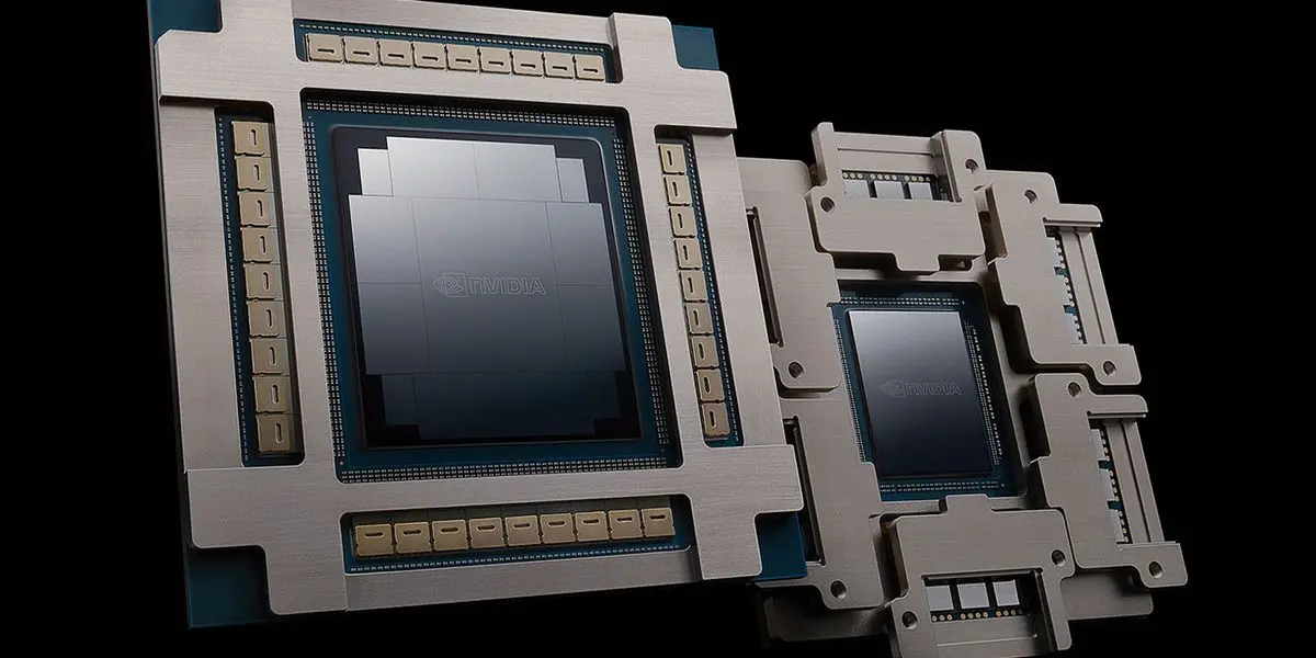
NVIDIA has just unveiled more details on its new Spectrum-X Ethernet Photonics interconnect, using next-gen silicon photonics replacing the traditional optical interconnect, and it's a "game changer" for AI. During the recent Hot Chips 2025 event, NVIDIA presented its next-gen Spectrum-X Ethernet Photonics interconnect, showing some rather huge improvements in scaling AI factories, and making sure the new interconnect will be an effective and powerful replacement of the traditional optical interconnect. NVIDIA went into detail about the need of co-packaged photonics, and how massively it can scale AI factories, with the company noting that AI factories use around 17x more optics power compared to a traditional cloud data center, mostly because of the increased in GPU clusters that need dozens of optical transistors in order to talk to other GPUs. This makes networking optics cost around 10% of the total compute power of an AI factory on their own, and with the amount of AI servers and AI clusters being made, purchased, and built, NVIDIA wants in on that business with the use of its powerhouse Spectrum-X Ethernet Photonics. NVIDIA's new Spectrum-X Ethernet Photonics is the world's first with 200G/SerDes co-packaged optics, which is the cutting-edge standard in electrical signaling. The new Spectrum-X Ethernet Photonics compared to pluggable transceivers, offer improved signal integrity and lower DSP requirements. This is because the photonic engine (PIC) is right beside the switch ASIC. This means there's no need for long PCB traces, as well as a massive decrease in laser counts, with a 1.6Tb/s link dropping from eight lasers down to just two, resulting in reduced power consumption and higher transfer reliability. NVIDIA's new CPO was co-invented with its ecosystem partners, with hundreds of patents and licensed to partners, with the Silicon Photonics CPO chip packing an ultra-high 1.6T transfer, with MRMs (Micro-Ring Modulators) on board. This results in higher bandwidth with a lower footprint and less power used. Spectrum-X Ethernet Photonics is also the world's first 3D-stacked silicon photonics engine made on TSMC, as NVIDIA partnered with TSMC on silicon photonics. NVIDIA's new silicon photonics inside of a data center is up to 3.5x more power efficient, 10x higher resoliency, and 1.3x faster time to operation compared to the optical standard. This is the game changer for AI compute, which can scale incredibly fast and high once silicon photonics is the mainstream interconnect. The company showed off a full-scale switch with integrated photonics, the new NVIDIA Spectrum-6 102T, the new flagship offering from NVIDIA. We can expect: * 2x throughput * 63x signal integrity * 4x fewer lasers * 1.6x bandwidth density * 13x better laser reliability * Replaces 64 separate transceivers NVIDIA's new foray into silicon photonics has been a long time coming, but its first steps are here with a bang. NVIDIA Photonics will feature radically reduced power consumption, easier scaling, and performance boosts in interconnect by using the power of photonics. Co-packaged silicon optics feature 3x higher GPU under ISO power and 4 x reduction in the lasers required. This means that there's far more power available to the chip, and can be moved away from networking to the actual clusters of GPU on the chip, providing more performance. The scale out of co-packaged optics networking switches to scale AI factories to millions of GPUs is coming, with new Spectrum-X Ethernet Photonics' roll out, with up to 512 ports of 800G
Share
Share
Copy Link
Nvidia announces plans to implement light-based communication between AI GPUs by 2026, introducing Quantum-X InfiniBand and Spectrum-X Ethernet platforms with co-packaged optics for improved efficiency and scalability in AI data centers.
Nvidia's Breakthrough in Silicon Photonics
Nvidia has announced plans to revolutionize AI data centers with the introduction of light-based communication between AI GPUs by 2026
1
. This groundbreaking technology, utilizing silicon photonics interconnects with co-packaged optics (CPO), aims to achieve higher transfer rates at reduced power consumption, addressing the growing demands of large-scale AI clusters.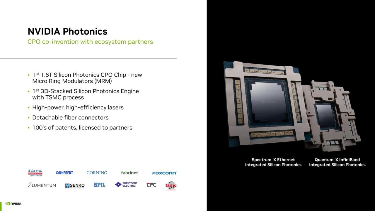
Source: TweakTown
The Need for Co-Packaged Optics
In large-scale AI clusters, thousands of GPUs must function as a unified system, presenting significant interconnection challenges. Traditional networking configurations using copper cables have become impractical for high speeds like 800 Gb/s, necessitating optical connections for nearly all server-to-switch and switch-to-switch links
1
.Advantages of Co-Packaged Optics
Nvidia's CPO technology offers substantial improvements over traditional pluggable optical modules:
- Reduced electrical loss from 22 decibels to 4 decibels
- Decreased per-port power consumption from 30W to 9W
- 3.5x increase in power efficiency
- 64x better signal integrity
- 10x boost in resiliency due to fewer active devices
- 30% faster deployment times
2
Quantum-X and Spectrum-X Platforms
Nvidia is set to introduce two major platforms leveraging CPO technology:
-
Quantum-X InfiniBand switches (early 2026):
- 115 Tb/s throughput
- 144 ports at 800 Gb/s each
- 14.5 TFLOPS of in-network processing
- Liquid-cooled design
1
-
Spectrum-X Ethernet Photonics (second half of 2026):
- Based on Spectrum-6 ASIC
- SN6810: 102.4 Tb/s bandwidth, 128 ports at 800 Gb/s
- SN6800: 409.6 Tb/s bandwidth, 512 ports at 800 Gb/s
- Liquid-cooled design
2
Source: Tom's Hardware
Impact on AI Data Centers
The implementation of CPO-based switches is expected to drive new AI clusters for generative AI applications. Key benefits include:
- Elimination of thousands of discrete components
- Faster installation and easier servicing
- Reduced power consumption per connection
- Improvements in time-to-turn-on and time-to-first-token metrics
- Enhanced long-term reliability
3
Related Stories
Collaboration with TSMC
Nvidia's development timeline aligns closely with TSMC's COUPE (Compact Universal Photonic Engine) roadmap, which unfolds in three stages:
- First generation: 1.6 Tb/s data transfer for OSFP connectors
- Second generation: 6.4 Tb/s at the motherboard level using CoWoS packaging
- Third generation: 12.8 Tb/s within processor packages
1
Future Implications
Source: Dataconomy
Nvidia emphasizes that co-packaged optics are not merely an optional enhancement but a fundamental requirement for future AI data centers. This technology is poised to be a game-changer in AI compute, enabling rapid and extensive scaling of AI factories. The company's foray into silicon photonics marks a significant step towards more efficient and powerful AI infrastructure, potentially reshaping the landscape of high-performance computing
3
.References
Summarized by
Navi
[2]
Related Stories
Nvidia Unveils Revolutionary Silicon Photonics Switches for AI Data Centers
19 Mar 2025•Technology
Nvidia Embraces Optical Technology for Networking, But Not Yet for GPUs
19 Mar 2025•Technology
Scintil Photonics begins shipping laser chips to customers, targets AI data center demand
12 Mar 2026•Technology

Recent Highlights


Recent Highlights
Today's Top Stories


Your Daily Dose of Curated AI News
Don’t drown in AI news. We cut through the noise - filtering, ranking and summarizing the most important AI news, breakthroughs and research daily. Spend less time searching for the latest in AI and get straight to action.