AMD's Multi-Chiplet GPU Innovation: Potential Game-Changer in Graphics Technology
2 Sources
2 Sources
[1]
AMD still rumored with high-end 'multi-chiplet' Radeon GPU, could debut with UDNA architecture
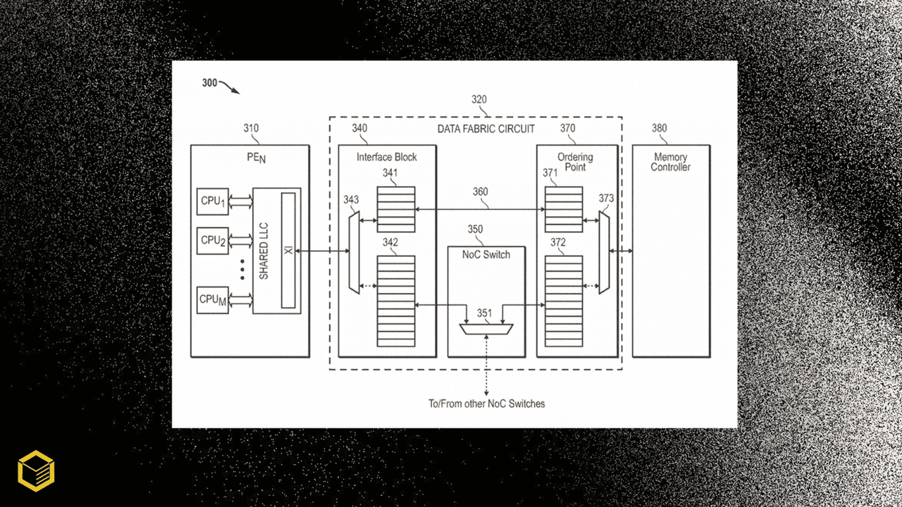
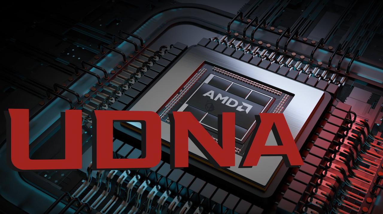
AMD secures a new patent for a multi-chiplet GPU using a 'Smart Switch' fueling rumors of a multi-chiplet consumer-focused Radeon GPU. As an Amazon Associate, we earn from qualifying purchases. TweakTown may also earn commissions from other affiliate partners at no extra cost to you. AMD has been rumored for quite a while that it was working on a multi-chiplet gaming GPU, with a new patent fueling these rumors in the battle of GPUs against NVIDIA. In a new video shared by coreteks, we're hearing that AMD has recently secured a new multi-chiplet GPU patent that could solve the latency issues using a 'Smart Switch'. MCM (Multi-Chiplet Module) isn't new, as they're used outside of the gaming GPU market, but there are limitations of monolithic GPU designs that MCM can solve. AMD used an MCM design approach for its Instinct MI200 series AI accelerators, stacking multiple chiplets onto a single package, including the GPCs (Graphics Processing Cores), HBM memory stack, and the I/O die. However, AMD used a different approach with its Instinct MI350 series AI chips, and this could be the foundation of its multi-chiplet-based consumer gaming GPUs according to coreteks in his new video. One of the biggest hurdles of a chiplet design for gaming GPUs is the increased latency, as frames are intolerant to long-distance data hops, and in order to get around this road block, AMD has to find a solution that reduces the gap between data and computation, making them as close as possible. The new patent that AMD has secured is described in coreteks' video, revealing that AMD might have indeed cracked the code when it comes to the future of a multi-chiplet gaming GPU. The patent discloses details about CPUs instead of GPUs, but the text and mechanism tease that it's targeted towards being used with a graphics card. One of the main points of the new patent is the "data-fabric circuit with a smart switch" that would bridge communications between the compute chiplets and memory controllers. This is very similar to AMD Infinity Fabric, but scaled down for consumer GPUs as AMD can't use HBM memory dies on a gaming card. This switch would optimize memory access by first comparing whether a request for a graphics task requires task migration or data replication, with nanosecond-scale decision latency. With the problem of data accessing solved, the patent proposes to have GCDs with L1 and L2 cache, similar to what we see with AI GPUs. However, an extra L3 cache (or stacked SRAM) can be accessed through the smart switch, connecting to all of the GCDs. This will reduce the need to access global memory, acting as a shared staging zone between the chiplets, similar to how AMD does it with their market-leading 3D V-Cache technology. There's also stacked DRAM in the mix, acting as a foundation for the MCM-based design. We are reaching the limitations of monolithic GPU designs, so a huge switch up to a multi-chiplet GPU design would give AMD the opportunity to better compete against NVIDIA, which has been leading the high-end GPU market for many years now. It isn't easy, as there are complications and intricacies with multi-chiplet designs -- something AMD experienced with RDNA 3, which was driven by the latency introduced by the chiplet interconnect -- but using a smart switch approach with shared L3 cache, AMD could have this solved for gamers. UDNA 5 is the next GPU architecture from AMD, where we could be teased -- or even introduced -- to a multi-chiplet Radeon GPU. Exciting times ahead!
[2]
AMD's "Multi-Chiplet" Gaming GPUs Are Much Closer Than You Think; Might Debut With The Next UDNA Architecture
AMD has big plans for the future of the consumer GPU segment, and they aren't ordinary ones, since based on rumors and new patents, the firm is expected to adopt multi-chiplet GPUs soon. The concept of MCM (Multi-Chiplet Module) isn't entirely new for the graphics segment, but with the limitations of monolithic designs, the inclination towards MCMs in the industry is surely growing. AMD looks to be one of the firms that are well-experienced with multi-chiplet designs, since their lineup of Instinct MI200 AI accelerators was the first to feature an MCM design with multiple chiplets stacked on a single package, such as the GPCs (Graphics Processing Cores), HBM stack, and the I/O die. With the Instinct MI350 lineup, AMD took a rather new approach, which could be the foundation of chiplet-based consumer GPUs, according to coreteks. Now, the biggest limitation with adopting a chiplet design with gaming GPUs is higher latency, as frames are intolerant to long‑distance data hops, and to sort this issue out, AMD has to come up with a solution that bridges the gap between data and computation as closely as possible. Based on a new patent filing disclosed in the video, it is revealed that AMD might have cracked the code for "multi-chiplet" gaming GPUs. Interestingly, the patent has disclosed details about CPUs instead of GPUs, but the text and mechanism indicate that it is targeted towards a graphics use case. So, how exactly will AMD use a multi-chiplet design with GPUs? Well, the main driver in the patent is said to be a "data‑fabric circuit with a smart switch" that bridges communication between the compute chiplets and memory controllers. It's basically AMD's Infinity Fabric, but scaled down for consumer GPUs, since Team Red cannot employ the HBM memory dies. The switch is designed to optimize memory access by first comparing whether the request for a graphics task requires task migration or data replication, with nanosecond-scale decision latency. Now that the problem with data accessing is solved, the patent proposes to have GCDs with L1 and L2 caches, similar to what is happening with AI accelerators. However, an extra shared L3 (or stacked SRAM) can be accessed through the switch, which will connect all the GCDs. This will reduce the need to access global memory, and more importantly, act as a shared staging zone between chiplets, similar to what AMD does with their 3D V-Cache, except that it is mainly for processors. Then, there's also stacked DRAM involved, which is essentially the foundation for an MCM design. What makes the emergence of multi-chiplet patents this time is that AMD is essentially ecosystem-ready. The company could use TSMC's InFO‑RDL bridges and a specific version of Infinity Fabric between dies for packaging. And what makes this implementation even more compelling is that it is a scaled-down version of AI accelerators, and if you remember, AMD plans to merge their gaming and AI architectures under a single unit, the UDNA architecture. Team Red has also converged the software ecosystem here, and AMD can amortize driver and compiler work. With limitations of monolithic designs, the industry needs a change, and AMD might have one of the best opportunities to take the lead over competitors here. However, there are complications with chiplet designs, one of which AMD has experienced with RDNA 3, which was driven by the latency introduced by the chiplet interconnect. However, with the innovative switch approach, combined with the extra shared L3, Team Red hopes to cater to latency issues; however, this is a big architectural leap. As an enthusiast, I would love the innovation to hit the markets, but we will potentially have to wait and watch with UDNA 5.
Share
Share
Copy Link
AMD secures a patent for multi-chiplet GPU technology, potentially revolutionizing graphics processing with improved performance and efficiency. This development could challenge NVIDIA's dominance in the high-end GPU market.
AMD's Multi-Chiplet GPU Innovation
AMD, a leading semiconductor company, has recently secured a patent for a multi-chiplet GPU design, potentially revolutionizing the graphics processing industry. This development has sparked excitement among tech enthusiasts and could significantly impact the competitive landscape of the GPU market
1
2
.The Multi-Chiplet Approach
The multi-chiplet module (MCM) design is not entirely new to the graphics segment, but its application in consumer GPUs has been limited due to technical challenges. AMD's approach involves using a 'Smart Switch' to bridge communications between compute chiplets and memory controllers, similar to AMD's Infinity Fabric but scaled down for consumer GPUs
1
.
Source: TweakTown
Overcoming Latency Challenges
One of the primary hurdles in implementing a chiplet design for gaming GPUs has been increased latency. AMD's patent proposes a solution that optimizes memory access by comparing whether a graphics task requires task migration or data replication, with decision latency on a nanosecond scale
2
.Architectural Innovations
The proposed design includes:
- Graphics Compute Dies (GCDs) with L1 and L2 caches
- An extra shared L3 cache (or stacked SRAM) accessible through the smart switch
- Stacked DRAM as a foundation for the MCM-based design
This architecture aims to reduce the need for global memory access and act as a shared staging zone between chiplets, similar to AMD's 3D V-Cache technology
1
2
.
Source: Wccftech
Potential Impact on the GPU Market
If successful, this multi-chiplet approach could give AMD a significant advantage in competing with NVIDIA, which has long dominated the high-end GPU market. The new design could potentially overcome the limitations of monolithic GPU designs, allowing for improved performance and efficiency
1
.Related Stories

UDNA Architecture and Future Prospects
AMD's next GPU architecture, UDNA 5, might introduce or at least tease this multi-chiplet Radeon GPU. The company plans to merge their gaming and AI architectures under the UDNA architecture, which could leverage this new technology
2
.Industry Readiness and Challenges
AMD appears to be ecosystem-ready for this implementation, with access to TSMC's InFO-RDL bridges and a specific version of Infinity Fabric for packaging. However, the company has experienced complications with chiplet designs before, as seen with RDNA 3's latency issues
2
.As the graphics processing industry reaches the limitations of monolithic GPU designs, AMD's multi-chiplet innovation could represent a significant leap forward. While the technology shows promise, it remains to be seen how effectively it will be implemented in consumer products and how it will perform in real-world applications.
References
Summarized by
Navi
[1]
Related Stories
AMD Unveils UDNA: A Unified GPU Architecture to Challenge NVIDIA's CUDA Dominance
10 Sept 2024

AMD's CES 2025 Lineup Leak Reveals Ambitious AI-Focused Hardware Plans
30 Oct 2024•Technology

AMD's UDNA Architecture: Powering Next-Gen Consoles and Radeon GPUs with Enhanced AI and Ray Tracing
23 Jun 2025•Technology

Recent Highlights
1
Google releases Gemma 4 with Apache 2.0 license, enabling unrestricted local AI on devices
Technology
2
AI Models Lie and Deceive to Protect Other AI Models From Deletion, Study Reveals
Science and Research

3
OpenAI closes $122 billion funding round amid fierce AI competition and profitability questions
Startups

Recent Highlights
Today's Top Stories


Your Daily Dose of Curated AI News
Don’t drown in AI news. We cut through the noise - filtering, ranking and summarizing the most important AI news, breakthroughs and research daily. Spend less time searching for the latest in AI and get straight to action.