AMD's 2nm Leap: Challenging Nvidia's AI GPU Dominance with Next-Gen Instinct MI450
4 Sources
4 Sources
[1]
AMD could beat Nvidia to launching AI GPUs on the cutting-edge 2nm node -- Instinct MI450 is officially the first AMD GPU to launch with TSMC's finest tech
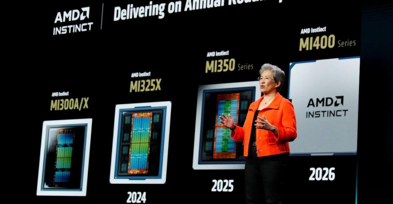
Compute chiplets of AMD's next-generation Instinct MI450-series accelerators based on the CDNA 5 architecture set to be introduced in the second half of next year will be made on TSMC's N2 (2nm-class) fabrication technology, marking the first time the company will use a leading-edge manufacturing process for AI GPUs. Usage of the latest production node could give AMD a major advantage when competing against Nvidia's upcoming Rubin GPUs and systems on their base, which are set to be made on N3. "We are really excited about our MI450 generation, it has 2nm technology, so the most advanced fabrication capability, it has rack scale solutions, so we are really putting all of these compute elements together," Lisa Su, chief executive of AMD, revealed in an interview with Yahoo Finance. "The way to think about it is it takes a village to build this all. So, you know, we are of course very, you know, proud and focused." AMD's current-generation CDNA 4-based Instinct MI350-series AI accelerators use compute chiplets produced by TSMC using one of its proven N3-series fabrication technologies (which entered mass production in late 2022), so it is reasonable for the company to transit to a 2nm-class manufacturing process for its next-generation GPUs for AI and HPC applications. AMD's Instinct MI450-series accelerators will be the company's first processors tailored specifically for AI and, therefore, support appropriate data formats and instructions. Perhaps, a new node will enable AMD to pack in some secret sauce into its new compute GPUs. Indeed, N2 promises tangible -- as TSMC calls them 'full node' -- improvements compared to predecessors, such as a 10% to 15% performance improvement at the same power or complexity, or a 25% to 30% power reduction at the same frequency, along with a 15% increase in transistor density compared to N3E. The key advantage of the new production node will be gate-all-around (GAA) transistors that enable developers to tailor designs for maximum efficiency when using design and technology co-optimization (DTCO). Overall, by migrating to N2, AMD will obtain a broad set of benefits that include performance efficiency and transistor density. Nvidia has already announced that its next-generation Rubin GPUs will be produced using one of TSMC's N3 technologies (presumably N3P tailored for Nvidia's needs), so AMD's Instinct MI450 will have an edge over its key rival when it comes to manufacturing process. AMD's Helios rack-scale solution with 72 Instinct MI450 GPUs will also carry more HBM4 memory (51TB vs 21TB) and offer more memory bandwidth (1,400 TB/s vs 936 TB/s) compared to Nvidia's Rubin-based NVL144 machine. However, Nvidia's next-generation rack-scale solution will offer tangibly higher FP4 (well, NVFP4) performance compared to AMD's Helios (3,600 PFLOPS vs 1,440 PFLOPS), so it remains to be seen which of the systems will be faster and more power efficient, especially given uncertainties with UALink scale-up interconnections for the Instinct MI450-series GPUs. One of the first customers to adopt AMD's Instinct MI450 is said to be OpenAI, which will start to get the hardware in the second half of next year, with AMD revenue ramping sharply afterward. The project will unfold over multiple phases and should generate double-digit billions in incremental sales once fully operational, according to Su. For AMD, the alliance signifies validation of years of investment in its AI architectures and data center solutions.
[2]
AMD taps TSMC's 2nm node to challenge Nvidia in next-gen AI compute
Serving tech enthusiasts for over 25 years. TechSpot means tech analysis and advice you can trust. What we know so far: AMD's new Instinct MI450 is a statement of intent. Built on the cutting-edge 2nm process and backed by a major partnership with OpenAI, the accelerator signals a turning point in how AI hardware is designed and scaled. The move puts fresh pressure on Nvidia and others to rethink their roadmaps, as the race to power ever-larger AI models pushes the limits of what silicon, and the industry, can deliver. AMD is staking its claim as a technological leader in AI hardware, confirming that its forthcoming MI450 accelerator will use an advanced 2-nanometer fabrication process - a significant leap ahead of rival Nvidia, whose next-generation Vera Rubin GPUs are expected to be built on a 3-nanometer node. The announcement came amid growing industry competition for powering increasingly complex artificial intelligence workloads. In a recent interview with Yahoo Finance following a high-profile partnership with OpenAI, AMD Chief Executive Lisa Su confirmed the 2nm milestone. According to Su, the MI450 accelerator, scheduled to be released in 2026, will incorporate the latest TSMC fabrication technology for its core computational die - a decision expected to deliver advancements in thermal efficiency and computing power. The 2nm process will be used exclusively for the MI450's Accelerator Core Die (XCD). Other components, including the Active Interposer Die (AID) and Media Interface Die (MID), will utilize TSMC's refined 3nm node, reflecting a hybrid approach to optimizing each segment of the GPU design for its specific computational role. This layered architecture combines ultra-dense, high-speed cores with robust interconnect and media handling subsystems, aiming to address AI workloads that demand massive parallel processing and efficient data movement at scale. Su detailed the magnitude of AMD's collaboration with OpenAI, describing a "six gigawatt" deployment that is expected to generate tens of billions of dollars in revenue over the next several years. According to the CEO, the deal will make OpenAI a lead customer for the MI450 generation. The scope of the initiative highlights the scale of AI infrastructure development underway globally. Su described the challenge of building out a multi-gigawatt computing backbone for the "next era" of artificial intelligence. She acknowledged that building millions of high-performance GPUs - each engineered with advanced silicon and supported by rack-scale integration - is an immense technical feat, touching everything from manufacturing capacity to energy infrastructure. Su also addressed broader industry concerns about potential risks or bottlenecks, noting that collaboration across the ecosystem, from chipmakers and cloud providers to government and enterprise, will be essential for scaling AI deployments. "This is one of those points in time where you need every part of the food chain to come together and say, 'we want to do this, we want to build fast, we want to build big,'" said Su.
[3]
Can AMD's 2nm AI chip finally challenge Nvidia's dominance?
AMD's 72-GPU Helios rack with MI450s will feature 51 TB of HBM4 memory significantly more than the 21 TB planned for Nvidia's competing Rubin system. AMD announced its next-generation Instinct MI450 AI accelerators, based on the CDNA 5 architecture, will be manufactured using TSMC's 2nm process technology. The accelerators are scheduled for introduction in the second half of next year. The use of TSMC's N2 fabrication process for the compute chiplets marks the first time AMD will employ a leading-edge manufacturing node for its AI GPUs. Lisa Su, chief executive of AMD, confirmed the technical details. "We are really excited about our MI450 generation, it has 2nm technology, so the most advanced fabrication capability, it has rack scale solutions, so we are really putting all of these compute elements together," Su stated. "The way to think about it is it takes a village to build this all. So, you know, we are of course very, you know, proud and focused." This move represents a planned technological progression. AMD's current-generation Instinct MI350-series accelerators, built on the CDNA 4 architecture, utilize compute chiplets produced on one of TSMC's N3-series technologies, which entered mass production in late 2022. The transition to a 2nm-class process for the next-generation GPUs is a sequential step. The Instinct MI450 series will also be AMD's first processors specifically tailored for artificial intelligence, incorporating support for dedicated AI data formats and instructions. TSMC's N2 node is designed to deliver "full node" improvements over its predecessors. The process offers a 10% to 15% performance increase at the same power and complexity, or a 25% to 30% reduction in power consumption at the same frequency. The N2 node also provides a 15% increase in transistor density compared to the N3E process. A key technological enabler is the use of gate-all-around (GAA) transistors, which allow developers to better tailor designs for maximum efficiency through design and technology co-optimization (DTCO). This migration to N2 provides AMD benefits across performance, efficiency, and density. AMD's manufacturing decision positions its product against upcoming hardware from competitor Nvidia. Nvidia has announced that its next-generation Rubin GPUs will be produced using one of TSMC's N3 technologies, likely the N3P process tailored for its requirements. This places AMD's Instinct MI450 on a more advanced manufacturing process compared to its rival's announced plans. A comparison of the companies' planned rack-scale solutions reveals further differences. AMD's Helios system, with 72 Instinct MI450 GPUs, will carry 51 TB of HBM4 memory and provide 1,400 TB/s of memory bandwidth. In contrast, Nvidia's Rubin-based NVL144 machine will have 21 TB of memory and 936 TB/s of bandwidth. Nvidia's system, however, is specified to offer higher FP4 performance, at 3,600 PFLOPS using its NVFP4 format, compared to the 1,440 PFLOPS for AMD's Helios. The final performance and efficiency of the systems will also depend on factors like the UALink scale-up interconnections for the MI450-series GPUs. OpenAI is reported to be one of the first customers to adopt the Instinct MI450, with hardware deliveries scheduled to begin in the second half of next year. Following this deployment, AMD anticipates a sharp revenue ramp-up. According to Su, the project will unfold over multiple phases and is projected to generate double-digit billions in incremental sales once fully operational. This alliance serves as a validation of AMD's investment into its AI architectures and data center solutions.
[4]
AMD's Lisa Su confirms next-gen GPUs are 2nm, beating NVIDIA's upcoming Vera Rubin
TL;DR: AMD will launch its next-generation MI450 AI accelerator in 2026 using advanced 2nm silicon technology, surpassing NVIDIA's upcoming 3nm Vera Rubin GPU. This smaller process promises improved efficiency and performance, strengthening AMD's competitive position in AI hardware amid its strategic partnership with OpenAI. AMD has scored one point over NVIDIA after company CEO Lisa Su confirmed that its next-generation MI450 AI accelerator will be built on a 2nm silicon process, beating NVIDIA's upcoming Vera Rubin architecture built on 3nm silicon. Skip to 12:49 for the interview with AMD's Lisa Su Su confirmed the nanometer size in a recent interview with Yahoo Finance, where she was discussing the recent partnership announcement with ChatGPT-creator OpenAI. For those who don't know, OpenAI and AMD recently announced a new partnership that involves AMD providing OpenAI with its next-generation GPUs until it has completed the agreed-upon 1 gigawatt of power. In exchange, AMD will provide OpenAI with approximately 10% of its company. During the interview, Su revealed that AMD's upcoming AI accelerator, scheduled for release in 2026, will utilize 2nm technology, which means it will leapfrog over 3nm. Notably, NVIDIA's upcoming next-generation AI GPU architecture, Vera Rubin, will utilize 3nm silicon, giving AMD a competitive edge over Team Green in this regard. Why does the nm matter? Typically, a reduction in silicon process size leads to performance gains in the form of increased efficiency and raw performance. Since AMD is using 2nm silicon, it will help the company compete with NVIDIA's next-generation AI products. Notably, reliable GPU leaker Kepler_L2 revealed that not all of AMD's Instinct MI450 GPU will be built on a 2nm process, as it will also use TSMC's N3P (3nm) silicon for its Active Interposer Die (AID) and Media Interface Die (MID). It will only be AMD's Accelerator Core Die (XCD) that will be built on TSMC's 2nm (N2) process.
Share
Share
Copy Link
AMD announces its upcoming Instinct MI450 AI accelerators will use TSMC's 2nm process, potentially outpacing Nvidia's next-gen 3nm GPUs. This technological advancement, coupled with a major partnership with OpenAI, signals AMD's strong push into the AI hardware market.
AMD's Technological Leap with 2nm AI Accelerators
AMD is set to make a significant technological advancement in the AI hardware market with its upcoming Instinct MI450 series accelerators. In a recent interview, AMD CEO Lisa Su confirmed that the compute chiplets of these next-generation AI GPUs will be manufactured using TSMC's N2 (2nm-class) fabrication technology
1
. This marks the first time AMD will utilize a leading-edge manufacturing process for its AI GPUs, potentially giving the company a competitive edge over its rival Nvidia.
Source: TweakTown
Performance and Efficiency Gains
TSMC's N2 process promises substantial improvements over its predecessors. These include a 10% to 15% performance boost at the same power or complexity, a 25% to 30% power reduction at the same frequency, and a 15% increase in transistor density compared to the N3E process
1
. The use of gate-all-around (GAA) transistors enables developers to optimize designs for maximum efficiency through design and technology co-optimization (DTCO).Hybrid Architecture and Memory Advantages
While the core compute die will use the 2nm process, AMD is adopting a hybrid approach for the MI450. The Active Interposer Die (AID) and Media Interface Die (MID) will utilize TSMC's refined 3nm node
2
. This layered architecture aims to optimize each segment of the GPU design for its specific computational role, addressing the demands of AI workloads that require massive parallel processing and efficient data movement at scale.
Source: Tom's Hardware
Comparison with Nvidia's Next-Gen GPUs
AMD's move to 2nm technology puts pressure on Nvidia, whose next-generation Rubin GPUs are expected to use one of TSMC's N3 technologies
3
. In terms of memory capabilities, AMD's 72-GPU Helios rack with MI450s will feature 51 TB of HBM4 memory and 1,400 TB/s of memory bandwidth, significantly surpassing the 21 TB and 936 TB/s planned for Nvidia's competing Rubin system3
.Strategic Partnership with OpenAI
AMD's technological advancements are complemented by a major partnership with OpenAI. The collaboration involves a "six gigawatt" deployment expected to generate tens of billions of dollars in revenue over the next several years
2
. This deal positions OpenAI as a lead customer for the MI450 generation, validating AMD's investments in AI architectures and data center solutions.Related Stories


Industry Implications and Challenges
The scale of AMD's AI infrastructure development highlights the growing demands of the AI industry. Su emphasized the need for collaboration across the ecosystem, including chipmakers, cloud providers, government, and enterprise, to scale AI deployments effectively
2
. The success of these next-generation AI accelerators will depend not only on raw performance metrics but also on factors such as energy efficiency, scalability, and software ecosystem support.Looking Ahead
With the Instinct MI450 series scheduled for introduction in the second half of 2026, AMD is positioning itself as a formidable competitor in the AI hardware market
4
. The combination of advanced 2nm technology, strategic partnerships, and innovative GPU design could potentially challenge Nvidia's current dominance in the AI accelerator space. As the race to power increasingly complex AI models intensifies, the industry eagerly awaits the real-world performance and adoption of these next-generation AI GPUs.🟡 chivalry=🟡'', 'References
Summarized by
Navi
[1]
Related Stories
Recent Highlights
1
Tennessee Teens Sue Elon Musk's xAI Over Grok AI-Generated Child Abuse Images
Policy and Regulation

2
Pentagon designates Palantir Maven AI as core US military system in major defense shift
Technology

3
Supermicro Co-Founder Indicted in $2.5 Billion Nvidia AI Chip Smuggling Scheme to China
Policy and Regulation
Recent Highlights
Today's Top Stories


Your Daily Dose of Curated AI News
Don’t drown in AI news. We cut through the noise - filtering, ranking and summarizing the most important AI news, breakthroughs and research daily. Spend less time searching for the latest in AI and get straight to action.