NVIDIA Unveils Futuristic Vision for AI Compute: Silicon Photonics and 3D Stacking
3 Sources
3 Sources
[1]
Nvidia's eyeing up ways to beef up its future AI chips with GPUs on top of GPUs and the power of light
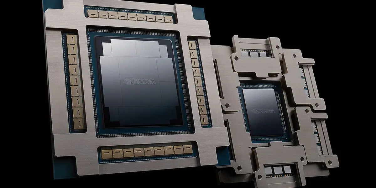
I'm not usually one for extravagant tech and hardware predictions -- things can change so much and so unpredictably that it's difficult to put too much weight behind such premonitions. But when it comes to AI tech, things move so quickly that what seems distant might not actually be too far away. Combine this with Nvidia being the one outlining the futuristic vision, and I take it a little more seriously. Nvidia's latest prediction, as outlined at the IEDM 2024 conference according to Dr. Ian Cutress (via TechPowerUp), is AI accelerators that are 3D-stacked and that use -- at least in part -- silicon photonics for data transmission. This is, as Cutress puts it, Nvidia's vision of "the future of AI compute". The image provided in the post shows an AI accelerator (ie, a datacentre GPU) that's split vertically into a substrate, integrated silicon photonics, GPU tiers, 3D stacked DRAM, and cold plate. The two big innovations in this picture, insofar as they could be applied to AI accelerators, are silicon photonics and the vertical stacking for logic. The former uses photons (light) to transmit data to and from optical components, which is faster and uses less power for more bandwidth than traditional electrical data transmission. Judging by the diagram, it looks like this light-based transmission technology would be used horizontally to connect to other accelerators. However, TechPowerUp says these accelerators feature "12 SiPh [silicon photonics] connections for intrachip and interchip connections, with three connections per GPU tile across four GPU tiles per tier". And "intra-chip connection" would seem to imply connection between each of these tiles within each tier, too. The diagram says there's an electrical (not optical) interconnect from die-to-die and tier-to-tier, which would suggest it's using more traditional Through-Silicon Via (TSV) tech to get the vertical stacking done. Silicon photonics is still only in its infancy. It might make more sense for Nvidia to use Through-Silicon-Via (TSV) technology for the vertical dimension, which essentially involves creating tiny tunnels as pathways between the stacked chips. This is the technology that allows the AMD Ryzen 7 9800X3D, for example, to have its processor sitting on top of its cache. Though usually we see 3D stacked chips limited to cache on logic, i.e. L3 cache on cores as per AMD's chip, rather than logic on logic, which is suggested here. It looks like four GPU tiles will exist per GPU "tier", and these tile tiers will be stacked vertically, too. Then on top of all of that, stacked DRAM. That all sounds like it'd get extremely toasty, and it's not something I'd expect to be achieveable in the immediate future. Whatever the case, it's certainly an interesting picture of what might be to come, and if anyone's able to do it it'll be Nvidia. And while we shouldn't infer too much about these technologies making their way across to gaming GPUs any time soon, it wouldn't be unreasonable to assume some of it might, at some point. If the technology's there and gets implemented in AI accelerators, the cheaper aspects (such as TSV stacking) might be worth adding to the consumer GPU mix. Gaming graphics doesn't require the kind of bandwidth that AI processing does, though, so I think we can remove photonics from the gaming equation for the foreseeable future. And these combined technologies won't even be possible for AI accelerators in the near future, either. I think Cutress is right: "My guess, 2028/2029/2030 minimum."
[2]
NVIDIA Presents The Future Of "AI Compute", Featuring Silicon Photonics & 3D GPU/DRAM Stacking
NVIDIA has presented its approach with next-gen AI accelerators, showcasing an innovative "silicon photonic" implementation at the IEDM 2024 conference. NVIDIA's Vision Of Next-Gen AI Accelerators Includes Utilizing Silicon Photonics Interposers & Unique Stacking Methods With modern-day packaging techniques, the industry has reached a point where there is a dire need for innovation, given that AI computing demands are increasing massively with time. Whenever there's a discussion about the future of packaging, silicon photonics (SiPh) is an approach deemed a viable alternative to conventional methods. Interestingly, at the IEDM 2024 conference, Team Green presented a unique strategy (via Ian Cutress) for next-gen accelerators, which involves using a SiPh interpose and stacking GPU tiles vertically for such a large compute product. Team Green's implementation proposes the integration of silicon photonics interposers, replacing the electrical interconnects out there. The utilization of SiPh brings in several benefits, likely in the form of providing higher bandwidth and lower latency, along with being a much more energy-efficient method than other methods. Not just the interposes, but NVIDIA plans to use 12 SiPh in intrachip and interchip communication, optimizing the data flow between individual GPU tiles, which is crucial for scalability and performance. Interestingly, the GPU stacking technique appeals the most in NVIDIA's vision, since the firm has revealed the use of "3D stacking", or stacking multiple GPU tiles vertically, to increase chip density and reduce footprint. Team Green calls this configuration a "GPU tier," with four GPU tiles in one tier, all stacked in a vertical orientation, to reduce interconnect latency and maybe implement power gating since this will be a possibility here. It will not just be GPUs, but NVIDIA will also 3D-stack DRAM chips, six per tile. While this sounds an optimistic approach, NVIDIA's vision holds several complexities, mainly with how "naive" silicon photonics technology actually is right now, given that it is a relatively newer standard. Team Green would need to see SiPh being in high-volume production before it sees any mainstream integration, and this happening will take a long time. Along with this, aggressive 3D stacking will make thermals a huge issue, forcing NVIDIA to integrate an intra-chip cooling solution, which hasn't surfaced up for now. The analyst Ian Cutress sees this implementation occurring within the next five years, likely between 2028 and 2030, given the complexities involved in this process.
[3]
NVIDIA shows off future of 'AI compute' with silicon photonics, 3D GPU + DRAM stacking
NVIDIA's vision of the future of AI compute has been teased: the AI GPU leader sees the use of a silicon photonics interposer, 3D stacked DRAM, and GPU 'tiers' that tease GPU on GPU tech in the future. In a new post on X from Ian Cutress, NVIDIA's vision of the future of AI compute has many different layers: module level cooling with a cold plate, die-to-die and tier-to-tier electrical connect, 3D stacked fine-grained DRAM, vertical power delivery, integrated silicon photonics, and an advanced package substrate. Cutress reports that NVIDIA teased the silicon photonics interposer, SiPh intrachip and interchip, 12 SiPh connects wth 3 per GPU tile, 4 GPU tiles per tier, GPU 'tiers' as the image above shows, and 3D stacked DRAM with 6 per tile, fine-grained. I do like the tease that NVIDIA plans to use 3D stacked GPUs, stacking multiple GPUs vertically, increasing chip density and reducing its footprint. With a "GPU tier" system using up to 4 GPU tiles per tier stacked vertically, reducing interconnect latency and probably using power gating as well. NVIDIA won't just be 3D stacking the GPUs, but would also use 3D-stacked DRAM chips with 6 per tile. An interesting, and exciting approach. Silicon photonics is still in its infancy, but TSMC has teased its next-gen COUPE technology using silicon photonics packaging which should be ready in 2026. We should expect NVIDIA's future of AI compute to roll out in the years after, between 2027 and 2030.
Share
Share
Copy Link
NVIDIA presents a groundbreaking concept for future AI accelerators, featuring silicon photonics and 3D stacking of GPUs and DRAM, potentially revolutionizing AI compute capabilities.

NVIDIA's Vision for Next-Generation AI Accelerators
NVIDIA, the leading AI GPU manufacturer, has unveiled its ambitious vision for the future of AI compute at the IEDM 2024 conference. This groundbreaking concept integrates advanced technologies such as silicon photonics and 3D stacking, potentially revolutionizing the landscape of AI hardware
1
2
.Silicon Photonics: The Future of Data Transmission
At the heart of NVIDIA's futuristic design is the implementation of silicon photonics (SiPh) technology. This innovative approach uses light (photons) for data transmission, offering significant advantages over traditional electrical methods:
- Increased speed and bandwidth
- Lower power consumption
- Improved efficiency in data transfer
The proposed design includes 12 SiPh connections for both intrachip and interchip communication, with three connections per GPU tile across four GPU tiles per tier
1
2
.3D Stacking: Vertical Integration for Enhanced Performance
NVIDIA's concept introduces a novel approach to GPU architecture through vertical stacking:
- Multiple GPU tiles stacked vertically, forming "GPU tiers"
- Four GPU tiles per tier, reducing interconnect latency
- 3D stacked DRAM, with six chips per tile
- Potential for power gating implementation
This vertical integration aims to increase chip density while reducing the overall footprint, potentially leading to significant performance improvements
2
3
.Challenges and Timeline
While NVIDIA's vision is ambitious, several challenges need to be addressed:
- Silicon photonics technology is still in its infancy
- Thermal management concerns due to aggressive 3D stacking
- Need for high-volume production of silicon photonics components
Experts, including analyst Ian Cutress, estimate that this technology might not be commercially viable until 2028-2030, given the complexities involved
1
2
3
.Related Stories
Implications for Consumer GPUs
While primarily focused on AI accelerators, some aspects of this technology could potentially trickle down to consumer GPUs in the future. However, gaming graphics may not require the extreme bandwidth provided by silicon photonics, making its implementation in consumer products less likely in the near term
1
.Industry Impact
NVIDIA's presentation of this futuristic AI compute vision underscores the company's commitment to pushing the boundaries of AI hardware. As AI computing demands continue to grow exponentially, innovations like these will be crucial in meeting future performance requirements and maintaining NVIDIA's leadership position in the AI hardware market
2
3
.References
Summarized by
Navi
[1]
[2]
Related Stories
Recent Highlights
1
AI chatbots validate you too much, making you less kind to others, Stanford study reveals
Science and Research

2
Anthropic's Claude Code Source Leak Reveals Hidden AI Agent Plans and Extensive System Access
Technology

3
Judge blocks Pentagon from branding Anthropic a security risk over AI safety guardrails dispute
Policy and Regulation


