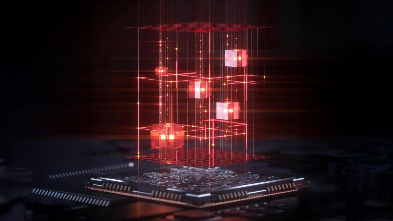
Photonic Chips: A Breakthrough in AI Processing and Energy Efficiency
8 Sources
8 Sources
[1]
Photonic chips provide a processing boost for AI
You have full access to this article via Jozef Stefan Institute. Systems based on artificial intelligence (AI) are becoming ever more widely used for tasks from decoding genetic data to driving cars. But as the size of AI models and the extent of their use grows, both a performance ceiling and an energy wall are looming. With the performance of transistors in computer chips set to plateau, the computing power needed to support AI models will push today's electronic hardware to its breaking point. Meanwhile, AI's overall energy demand is soaring, increasing carbon emissions and putting strain on local electricity grids around data centres. In September last year, technology firm Microsoft signed up for exclusive rights to the output of an entire US nuclear-power station to help to fuel its AI ambitions. To enable a more sustainable future, the fundamental data-processing hardware requires a radical overhaul. Writing in Nature, Hua et al. and Ahmed et al. demonstrate complementary breakthroughs using silicon photonics -- semiconductor chips that process light, rather than electricity -- to increase computational performance, while decreasing energy consumption. Their electronic-photonic computing systems have key performance metrics that are comparable to, and in some cases surpass, purely electronic processors in real-world applications. This represents a significant leap towards finally capitalizing on the promise of photonic computing. Photonic computing has been a topic of scientific research for decades, but real-world implementations have been held back by the lack of chip-scale, scalable optical analogues of the wildly successful silicon electronic integrated circuit. That has begun to change over the past decade, however, with the fabrication of high-performance photonic integrated circuits on the same silicon wafers as those used for microelectronics, largely motivated by the need for optical chip-to-chip interconnects. Although several state-of-the-art demonstrations have shown the potential of integrated photonics to accelerate computation, they have evaluated the performance of the photonic chips largely in isolation. But data in most real-world systems originate in the electronic domain, and so photonic computing requires close integration and co-design with electronics. Indeed, the two technologies are complementary, rather than direct competitors. In particular, photonics performs linear operations, in which there is a simple proportional relationship between input and output data, more efficiently than electronics does. Electronics, meanwhile, excels at non-linear operations, in which the input and output data are related by more complex mathematical functions that do not preserve a proportional relationship between the two. Photonic computing is particularly valuable for performing matrix multiplications, often referred to as multiply-accumulate (MAC) operations. These form the mathematical foundation of artificial neural networks and of many combinatorial optimization problems, which pop up frequently in areas such as resource allocation, network design, scheduling and supply-chain logistics. Solving such problems efficiently is a central priority for many modern computing systems, and is generally done by dedicated electronic computing accelerators, such as graphics processing units (GPUs) and tensor processing units (TPUs). These have highly parallel architectures that are better suited to calculating MAC operations than is the serial processing architecture of conventional central processing units (CPUs). The latest work shows that silicon photonic computing can provide drastic improvements in key performance metrics while consuming less energy and being fully capable of running standard AI workloads. Hua et al., a Singapore-based team at the company Lightelligence, target combinatorial optimization problems, whereas Ahmed et al., at the firm Lightmatter in Mountain View, California, focus on running state-of-the-art AI workloads such as large language models. Hua and colleagues apply their Photonic Arithmetic Computing Engine (PACE) to solve a class of combinatorial optimization challenges known as Ising problems, which have broad application in many real-world areas, including logistics and scheduling optimization. They directly compare its performance with that of a state-of-the-art NVIDIA A10 GPU for an Ising model that involves multiplying 64 × 64 matrices, and demonstrate a nearly 500-fold reduction in minimum latency -- a key metric of computational speed -- from 2,300 nanoseconds to just 5 nanoseconds. Furthermore, PACE has a latency scaling factor that is about 1,000 times smaller than that of TPUs, meaning that the performance gains in latency become even more pronounced as the matrix size is increased. Ahmed and colleagues, meanwhile, demonstrate a photonic processor that can execute standard state-of-the-art AI models -- including the natural language processor BERT and convolutional neural network ResNet, used mainly for image recognition -- with an accuracy close to that of standard electronic processors. The authors apply their photonic processor to an impressive breadth of real-world AI applications, including generating Shakespeare-like text, classifying film reviews as positive or negative and even playing the video game Pac-Man (Fig. 1). Despite these impressive breakthroughs, hurdles must still be overcome to realize the full potential of photonic computing as a commercial alternative to electronic accelerators. Much of the physical advantage of optical computing lies in its superior bandwidth and capacity for massive parallelism. Both current demonstrations are limited by a clock speed -- the number of operations that a processor can perform in one second -- of the order of 1 gigahertz, whereas optical architectures and photonic devices can support speeds in excess of 100 gigahertz with minimal power dissipation. Furthermore, both demonstrations use monochromatic light in a single spatial waveguide mode. This leaves plenty of room for future improvements that could use many frequency and spatial modes in parallel. Finally, it remains to be seen whether these systems can maintain performance when they are scaled to the complex and dynamic workloads of commercial AI deployments. Nevertheless, there are many reasons to expect that photonic computing accelerators will find their way into real-world systems in the near future. Crucially, the photonic and electronic chips used in both of these demonstrations were fabricated in standard, complementary metal-oxide-semiconductor (CMOS) foundries used to make microelectronic chips, and so this existing infrastructure can be immediately exploited to scale up manufacturing. Furthermore, both systems were fully integrated in a standard 'motherboard' interface, technically known as a peripheral component interconnect express interface, making them readily compatible with existing interfaces and protocols. Photonic computing has been in the making for decades, but these demonstrations might mean that we are finally about to harness the power of light to build more-powerful and energy-efficient computing systems.
[2]
Universal photonic artificial intelligence acceleration - Nature
You have full access to this article via Jozef Stefan Institute. With the exponential growth in AI model complexity driven by large language models, reinforcement learning and convolutional neural networks, electronic computers are now fundamentally bound by Moore's law and Dennard scaling. Photonics offers an alternative by exploiting the high bandwidth, low latency and energy efficiency of light-based computation. Recent developments, including photonic accelerators based on interleaved time-wavelength modulation and photoelectric multiplication, underline the progress towards photonic processors for AI. Although these systems have demonstrated essential linear algebra operations, such as matrix multiplication, challenges in achieving precision, scalability, system integration and compatibility with advanced AI architectures remain. Addressing these challenges is crucial for positioning photonic processors as a viable alternative to electronic accelerators, with the potential for substantial gains in computational speed and energy efficiency. Here we report the first photonic processor, to our knowledge, capable of executing state-of-the-art neural networks, including transformers, convolutional networks classification and segmentation, and reinforcement learning algorithms. Critically, this photonic processor achieves accuracies approaching those of 32-bit digital floating-point systems on advanced tasks, validating its computational integrity even without requiring advanced techniques such as fine-tuning and quantization-aware training. The design integrates six chips in a single package, using high-speed interconnects between vertically aligned photonic tensor cores (PTCs) and control dies, thus achieving high efficiency and scalability for AI computation. This work focuses on accurately executing state-of-the-art neural networks -- even with several hardware non-idealities discussed in the Supplementary information, the photonic processor generates 65.5 trillion adaptive block floating-point (ABFP) 16-bit operations per second at 78 W of electrical power and 1.6 W of optical power. This work represents the highest level of integration achieved in photonic processing. The photonic processor, depicted in Fig. 1a, integrates four 128 × 128 PTCs fabricated using GlobalFoundries' 90-nm photonics process, as illustrated in Fig. 1b. Each PTC occupies 14.00 × 24.96 mm and contains all photonic components and analogue mixed-signal circuits required to operate them, except for high-speed analogue-to-digital converters (ADCs). The processor also incorporates two digital control interface (DCI) chips, manufactured with GlobalFoundries' 12-nm process, each measuring 31.4 × 25.0 mm. High-speed ADCs are included in the DCI. This innovative package assembles six chips: two full-reticle, 25-billion-transistor DCI dies on an organic interposer (54 × 56 mm) with four PTC dies underneath (see Supplementary information section III). Figure 1c shows the DCI die floor plan. During a tensor operation, vectors flow from the input pipeline through a PTC to the output pipeline. The PTC floor plan is mirrored about the y axis to match two PTCs to one DCI. Each DCI includes 64 reduced instruction set computer (RISC) cores, implemented using quad-core 32-bit RISC-V SiFive E76-MC complexes and a 268-MB unified buffer for storing activations, weight parameters and other data. The PTC floor plan in Fig. 1d includes 128 10-bit photonic vector units and 128 × 128 7-bit weight unit cells.
[3]
New computer chips do math with light
Two tech companies have unveiled computer components that use laser light to process information. These futuristic processors could soon solve specific real-world problems faster and with lower energy requirements than conventional computers. The announcements, published separately April 9 in Nature, mark a major leap forward for this alternative approach to computing. Lightelligence, based in Boston, and Lightmatter, in Mountain View, Calif., have shown that light-based, or photonic, components "can do things that we care about, and that they can do them better than electronic chips that we already have," says Anthony Rizzo, a photonics engineer at Dartmouth College who was not involved in either study. Lasers already zap data across the world via fiber optic cables, and photonics plays a role in moving data in advanced data centers. In March, for example, tech company NVIDIA, based in Santa Clara, Calif., announced new technology that uses light to communicate between devices. But, Rizzo says, these light beams don't compute anything. Inside a conventional computer, incoming light signals are transformed into slower electronic 1s and 0s that move through tiny transistors. In contrast, light inside the Lightmatter and Lightelligence devices "is actually doing math," Rizzo says. Specifically, both use light to perform matrix multiplication, a fundamental operation in most AI processing as well as other areas of computing. In both new devices, all other calculations occur in electronic components. The timing of these new developments is crucial. AI models are growing in size and complexity, while the progress of traditional chips is slowing. Historically, the number of transistors that engineers could squeeze onto chips would roughly double every two years, a trend known as Moore's law. Tinier transistors meant faster, cheaper computing. But Moore's law has reached its limit, says Nick Harris, founder and CEO of Lightmatter. Other experts agree. The physics of how electricity moves through transistors prevents them from shrinking much further. Computers based on regular electronic chips "are not going to be getting better," Harris says. Photonic computing offers a potential solution. The Lightelligence device, named PACE, combines a photonic and electronic chip to speed up computation for optimization problems, which are crucial for industries such as finance, manufacturing and shipping. The Lightmatter device, on the other hand, is a more general-purpose processor that integrates four light-based and two electronic chips. The team used this system to run mainstream AI technology, including large language models like those behind ChatGPT or Claude. They also ran a deep learning algorithm that practiced playing Atari games, including Pac-Man. "That's never been done" using any sort of alternative computer processing technology, Harris says. Engineers had previously built experimental photonic processors that could do math, but these never came close to matching a regular computer's performance on real-world computing problems. One big problem with experimental photonic processors has been accuracy. Light signals can take on a vast range of values instead of representing just 1 and 0. If one of these values isn't transmitted correctly, a tiny mistake could compound into a big error in calculations. In the optimization problems Lightelligence tested, some randomness can be a good thing. It helps the system explore solutions more efficiently, the company said in a statement. Lightmatter addresses this issue by stacking electronic chips atop its photonic ones to carefully control the incoming and outgoing data, thus reducing errors. Their new processor "is not a lab prototype," Harris says. "This is a new type of computer. And it's here." The photonic components for both devices can be manufactured using the same factories and processes that already produce electronic chips, Rizzo says. So the technology will scale easily. "These could be in real systems very soon," he says, adding that the technologies could show up in data centers within five years.
[4]
Next generation computer chips could process data at the speed of light - new research
Electronic microchips are at the heart of the modern world. They're found in our laptops, our smartphones, our cars and our household appliances. For years, manufacturers have been making them more powerful and efficient, which increases the performance of our electronic devices. But that trend is now faltering because of the increased cost and complexity of manufacturing chips, as well as performance limits set by the laws of physics. This is happening just as there's a need for increased computing power because of the boom in artificial intelligence (AI). An alternative to the electronic microchips we currently use are photonic chips. These use light instead of electricity to achieve higher performance. However, photonic chips have not yet taken off due to a number of hurdles. Now, two papers published in Nature address some of these roadblocks, offering essential stepping stones to achieving the computing power required by complex artificial intelligence systems. By using light (photons) instead of electricity (electrons) for the transport and processing of information, photonic computing promises higher speeds and greater bandwidths with greater efficiency. This is because it does not suffer from the loss of electrical current due to a phenomenon known as resistance, as well as unwanted heat loss from electrical components. Photonic computing is also particularly suited for performing what are known as matrix multiplications - mathematical operations that are fundamental to AI. Those are some of the benefits. The challenges, however, are not trivial. In the past, the performance of photonic chips has generally been studied in isolation. But because of the dominance of electronics in modern technology, photonic hardware will need to be integrated with those electronic systems. However, converting photons into electrical signals can slow down processing times since light operates at higher speeds. Photonic computing is also based around analogue operations rather than digital ones. This can reduce precision and limit the type of computing tasks that can be carried out. It's also difficult to scale them up from small prototypes because large-scale photonic circuits cannot currently be fabricated with sufficient accuracy. Photonic computing will require its own software and algorithms, compounding the challenges of integration and compatibility with other technology. The two new papers in Nature address many of these hurdles. Bo Peng, from Singapore-based company Lightelligence, and colleagues demonstrate a new type of processor for photonic computing called a Photonic Arithmetic Computing Engine (Pace). This processor has a low latency, which means that there is a minimal delay between an input or command and the corresponding response or action by the computer. The large-scale Pace processor, which has more than 16,000 photonic components, can solve difficult computing tasks, demonstrating the feasibility of the system for real world applications. The processor shows how integration of photonic and electronic hardware, accuracy, and the need for different software and algorithms can be resolved. It also demonstrates that the technology can be scaled up. This marks a significant development, despite some speed limitations of the current hardware. In a separate paper, Nicholas Harris, from California-based company Lightmatter, and colleagues describe a photonic processor that was able to run two AI systems with accuracy similar to those of conventional electronic processors. The authors demonstrated the effectiveness of their photonic processor through generating Shakespeare-like text, accurately classifying movie reviews and playing classic Atari computer games such as Pac-Man. The platform is also potentially scalable, though in this case limitations of the materials and engineering used curtailed one measure of the processor's speed and its overall computational capabilities. Both teams suggest that their photonic systems can be part of scalable next generation hardware that can support the use of AI. This would finally make photonics viable, though further refinements will be needed. These will involve the use of more effective materials or designs.
[5]
US firm's light-powered computer tackles energy-hungry AI problems
Connection speeds are a great matter of concern when it comes to artificial intelligence due to its complex software. This complexity requires the software to be spread over many computers. Currently valued at $4.4 billion after a venture capital round of $850 million, Lightmatter is confident that it can use beams of light to process the computation itself. The company focused on this idea in a paper it published in the scientific journal Nature on Wednesday. Conventional computers use transistors that are similar to tiny on-off electrical switches. If the transistors are small, they generally gain more computing power. The chip industry hasn't seen exactly 'memorable moments' with its struggle in shrinking the size of these transistors. Lightmatter's chip avoids those challenges by using precisely calibrated beams of light, which it directs to interact with each other. The outcomes are measured using an integrated chip package manufactured in partnership with GlobalFoundries. Previously, photonic computers faced issues with precise computation. If the outcome of a computation was a very small number, the chip would report the answer as zero. Lightmatter solved the issue by grouping extremely large and small numbers before sending them through the photonic circuits, ensuring that the very small numbers aren't lost in the process.
[6]
Photonic chips boost computing speed and efficiency to address growing demand
Computer chips that combine the use of light and electricity are shown to increase computational performance, while reducing energy consumption, compared with conventional electronic chips. The photonic computing chips, described in two papers in Nature this week, might address the growing computing demands driven by advancing artificial intelligence technology. The growth in the complexity of artificial intelligence and deep learning models is pushing conventional electronic computing to its limits and has ever-increasing energy demands. Photonic computing, which uses photons rather than electrons, presents a potential solution to these challenges. Multiplication and accumulation -- central computational operations for artificial intelligence -- can be performed faster and more efficiently using photonics circuits. Such advantages have been difficult to demonstrate in hardware that integrates photonic chips into conventional electronics, but two new papers probe the performance of photonic computing chips integrated with silicon electronics. Bo Peng and colleagues demonstrate a photonic accelerator, called PACE, that allows very low latency computing, a measure of computational speed that is important for real-time processing. The large-scale accelerator, comprising more than 16,000 photonic components in a 64 x 64 matrix, enables high-speed computing (up to 1 GHz) and demonstrates up to a 500-fold reduction in minimal latency compared with small-scale circuits or single photonic components. PACE is shown to solve hard computational problems known as Ising problems, demonstrating the feasibility of the system for real-world applications. In an independent paper, Nicholas Harris and colleagues describe a photonic processor that can efficiently implement AI models with high accuracy. The processor, which consists of four 128 x 128 matrices, can execute the natural language processing model BERT and a neural network called ResNet (used for image processing) at accuracies similar to those of conventional electronic processors. The authors show that their photonic processor has a range of applications, including generating Shakespeare-like text, accurately classifying movie reviews, and playing classic Atari computer games such as Pac-Man. Both teams suggest that their systems are scalable, though further optimization is needed. "Photonic computing has been in the making for decades, but these demonstrations might mean that we are finally about to harness the power of light to build more-powerful and energy-efficient computing systems," notes Anthony Rizzo in an accompanying News & Views article.
[7]
Leveraging silicon photonics for scalable and sustainable AI hardware
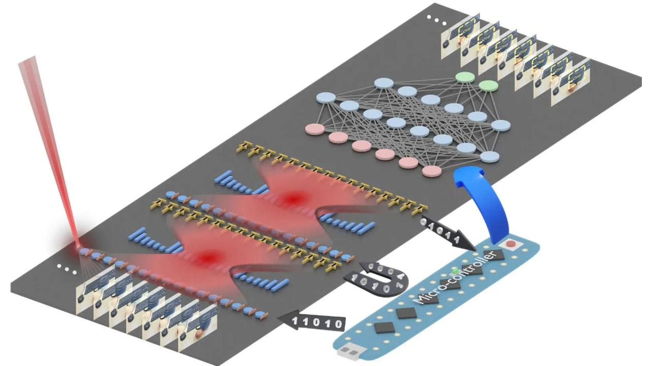
The emergence of AI has profoundly transformed numerous industries. Driven by deep learning technology and Big Data, AI requires significant processing power for training its models. While the existing AI infrastructure relies on graphical processing units (GPUs), the substantial processing demands and energy expenses associated with its operation remain key challenges. Adopting a more efficient and sustainable AI infrastructure paves the way for advancing AI development in the future. A recent study published in the IEEE Journal of Selected Topics in Quantum Electronics demonstrates a novel AI acceleration platform based on photonic integrated circuits (PICs), which offer superior scalability and energy efficiency compared to conventional GPU-based architectures. The study, led by Dr. Bassem Tossoun, a Senior Research Scientist at Hewlett Packard Labs, demonstrates how PICs leveraging III-V compound semiconductors can efficiently execute AI workloads. Unlike traditional AI hardware that relies on electronic distributed neural networks (DNNs), photonic AI accelerators utilize optical neural networks (ONNs), which operate at the speed of light with minimal energy loss. "While silicon photonics are easy to manufacture, they are difficult to scale for complex integrated circuits. Our device platform can be used as the building blocks for photonic accelerators with far greater energy efficiency and scalability than the current state-of-the-art," explains Dr. Tossoun. The team used a heterogeneous integration approach to fabricate the hardware. This included the use of silicon photonics along with III-V compound semiconductors that functionally integrate lasers and optical amplifiers to reduce optical losses and improve scalability. III-V semiconductors facilitate the creation of PICs with greater density and complexity. PICs utilizing these semiconductors can run all operations required for supporting neural networks, making them prime candidates for next-generation AI accelerator hardware. The fabrication started with silicon-on-insulator (SOI) wafers that have a 400 nm-thick silicon layer. Lithography and dry etching were followed by doping for metal oxide semiconductor capacitor (MOSCAP) devices and avalanche photodiodes (APDs). Next, selective growth of silicon and germanium was performed to form absorption, charge, and multiplication layers of the APD. III-V compound semiconductors (such as InP or GaAs) were then integrated onto the silicon platform using die-to-wafer bonding. A thin gate oxide layer (Al₂O₃ or HfO₂) was added to improve device efficiency, and finally a thick dielectric layer was deposited for encapsulation and thermal stability. "The heterogeneous III/V-on-SOI platform provides all essential components required to develop photonic and optoelectronic computing architectures for AI/ML acceleration. This is particularly relevant for analog ML photonic accelerators, which use continuous analog values for data representation," Dr. Tossoun notes. This unique photonic platform can achieve wafer-scale integration of all of the various devices required to build an optical neural network on one single photonic chip, including active devices such as on-chip lasers and amplifiers, high-speed photodetectors, energy-efficient modulators, and nonvolatile phase shifters. This enables the development of TONN-based accelerators with a footprint-energy efficiency that is 2.9 × 10² times greater than other photonic platforms and 1.4 × 10² times greater than the most advanced digital electronics. This is indeed a breakthrough technology for AI/ML acceleration, reducing energy costs, improving computational efficiency, and enabling future AI-driven applications in various fields. Going forward, this technology will enable datacenters to accommodate more AI workloads and help solve several optimization problems. The platform will be addressing computational and energy challenges, paving the way for robust and sustainable AI accelerator hardware in the future.
[8]
New IEEE study explores AI acceleration with photonics
As the demand for artificial intelligence (AI) accelerates across industries, a new study published by the IEEE Photonics Society highlights a promising hardware breakthrough designed to address AI's growing energy and performance challenges. The research, led by Dr. Bassem Tossoun, Senior Research Scientist at Hewlett Packard Labs, introduces a photonic integrated circuit (PIC) platform that could reshape how AI workloads are processed. Unlike traditional GPU-based systems that rely on electronic distributed neural networks (DNNs), this new platform leverages optical neural networks (ONNs), operating at the speed of light with significantly reduced energy consumption. Published in the IEEE Journal of Selected Topics in Quantum Electronics, the study presents photonic acceleration as a scalable and sustainable alternative for next-generation AI hardware. The approach focuses on integrating photonic devices directly onto silicon chips using a mix of silicon photonics and III-V compound semiconductors. Silicon photonics technology has long been considered promising for data-heavy applications. However, scalability for complex AI operations remained a hurdle. The IEEE research team addressed this by combining silicon photonics with III-V materials such as indium phosphide (InP) and gallium arsenide (GaAs), enabling on-chip lasers, amplifiers, and high-speed optical components to function together efficiently. "Our device platform can be used as the building blocks for photonic accelerators with far greater energy efficiency and scalability than the current state-of-the-art," said Dr. Tossoun. The fabrication process began with silicon-on-insulator (SOI) wafers and incorporated a series of advanced steps, including lithography, doping, selective silicon and germanium growth, and die-to-wafer bonding for III-V materials. The result is a wafer-scale integration of critical components like on-chip lasers, amplifiers, modulators, photodetectors, and non-volatile phase shifters -- all essential for building optical neural networks. This level of integration allows the platform to execute AI and machine learning workloads with higher efficiency while minimizing energy losses commonly seen in electronic-based systems. DeepL named to Forbes AI 50 List for second consecutive year The new photonic platform is designed to support the growing infrastructure needs of datacenters running AI workloads. With its ability to handle intensive computational tasks more efficiently, the platform could help organizations optimize power usage while scaling AI operations. Looking ahead, the researchers see this innovation contributing to more sustainable AI development, helping overcome the rising energy demands of deep learning and large-scale data processing. The research is detailed in the paper titled "Large-Scale Integrated Photonic Device Platform for Energy-Efficient AI/ML Accelerators," published in the IEEE Journal of Selected Topics in Quantum Electronics. The project reflects ongoing efforts within the photonics community to develop hardware solutions that align with the future performance and sustainability needs of AI infrastructure.
Share
Share
Copy Link
Two tech companies, Lightelligence and Lightmatter, have unveiled photonic processors that use light for computation, potentially revolutionizing AI processing with increased speed and energy efficiency.

Photonic Computing: A New Era for AI Processing
In a significant leap forward for artificial intelligence (AI) processing, two tech companies have unveiled photonic processors that use light instead of electricity for computation. This breakthrough, detailed in separate publications in Nature, addresses the growing challenges of energy consumption and performance limitations in traditional electronic chips
1
2
.The Promise of Photonic Computing
Photonic computing offers several advantages over conventional electronic processors:
- Higher speeds and greater bandwidths
- Improved energy efficiency
- Reduced heat generation
- Particular suitability for matrix multiplications, fundamental to AI processing
3
As AI models grow in complexity and size, the limitations of traditional electronic chips become more apparent. Moore's Law, which has driven chip development for decades, is reaching its physical limits
4
. Photonic computing presents a potential solution to these challenges.Breakthrough Achievements
Two companies have made significant strides in photonic computing:
-
Lightelligence: Developed the Photonic Arithmetic Computing Engine (PACE), which demonstrates:
- Nearly 500-fold reduction in minimum latency compared to state-of-the-art GPUs
- Efficient solving of combinatorial optimization problems
1
-
Lightmatter: Created a more general-purpose processor that:
- Executes state-of-the-art neural networks, including transformers and convolutional networks
- Achieves accuracies approaching 32-bit digital floating-point systems
- Generates 65.5 trillion adaptive block floating-point (ABFP) 16-bit operations per second
2
5
Real-World Applications
The Lightmatter processor has demonstrated impressive capabilities in various AI applications:
- Generating Shakespeare-like text
- Classifying movie reviews
- Playing video games like Pac-Man
3
5
These achievements showcase the potential of photonic processors to handle complex AI workloads with high accuracy and efficiency.
Overcoming Challenges
Previous attempts at photonic computing faced several hurdles, including:
- Integration with existing electronic systems
- Accuracy and precision issues
- Scalability limitations
- Software and algorithm compatibility
3
4
Both Lightelligence and Lightmatter have addressed these challenges through innovative designs and integration techniques, paving the way for practical applications of photonic computing.
Related Stories
Manufacturing and Scalability
A crucial advantage of these new photonic processors is their compatibility with existing chip manufacturing processes. This compatibility allows for easier scaling and integration into current technology ecosystems
3
. Industry experts suggest that these photonic systems could be implemented in data centers within the next five years3
.Future Implications
The development of photonic processors has significant implications for the future of computing and AI:
- Potential to overcome the limitations of Moore's Law
- Increased processing power for complex AI models
- Reduced energy consumption in data centers and AI applications
- Acceleration of AI research and development
4
5
As the technology matures, we can expect to see further refinements in materials and designs, leading to even more powerful and efficient photonic computing systems
4
. This breakthrough marks a significant step towards a new era of computing, one that could revolutionize AI processing and pave the way for more advanced and energy-efficient technologies.References
Summarized by
Navi
[3]
[4]
[5]
Related Stories
MIT Develops Ultrafast Photonic Chip for AI Computations with Extreme Energy Efficiency
03 Dec 2024•Technology

Revolutionary Light-Based AI Chip: Smaller Than a Speck of Dust, Faster Than Traditional Computing
08 Feb 2025•Technology

Revolutionary Light-Powered Chip Boosts AI Efficiency 100-Fold
09 Sept 2025•Science and Research
Recent Highlights
1
AI chatbots validate you too much, making you less kind to others, Stanford study reveals
Science and Research

2
Anthropic's Claude Code Source Leak Reveals Hidden AI Agent Plans and Extensive System Access
Technology

3
Judge blocks Pentagon from branding Anthropic a security risk over AI safety guardrails dispute
Policy and Regulation

Recent Highlights
Today's Top Stories


Your Daily Dose of Curated AI News
Don’t drown in AI news. We cut through the noise - filtering, ranking and summarizing the most important AI news, breakthroughs and research daily. Spend less time searching for the latest in AI and get straight to action.