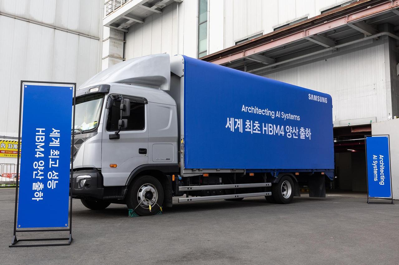
Samsung and Micron begin shipping HBM4 memory as race for AI acceleration hardware intensifies
15 Sources
15 Sources
[1]
Samsung and Micron start shipping HBM4
This bodes well for Nvidia getting Vera Rubin out the door next quarter as planned Samsung and Micron say they've started shipping HBM4 memory, the faster and denser RAM needed to power the next generation of AI acceleration hardware. Samsung yesterday announced it has begun mass production of HBM4 and even shipped some to an unnamed customer - probably Nvidia, which has confirmed its forthcoming Vera Rubin kit will use the memory. The Korean giant says its memory delivers a consistent processing speed of 11.7 gigabits-per-second, but users can juice that to hit 13Gbps under some circumstances. Total memory bandwidth can reach 3.3 terabytes-per-second in a single stack. For now, Samsung can sell this stuff in capacities between 24 and 36 gigabytes, but already plans to reach 48GB. Memory is so hot right now, but Samsung claims it has enhanced thermal resistance by 10 percent and heat dissipation by 30 percent, compared to HBM3E. The company also claims this new memory is 40 percent more energy efficient, meaning this kit uses less electricity and runs cooler, suggesting users can look forward to slower growth in their energy bills. The Korean giant didn't say what it will charge for this memory, an item of interest given soaring memory prices. But it did forecast its HBM sales will more than triple in 2026 compared to 2025, and that it expects to ship samples of HBM4E in the second half of 2026. Samsung claimed it is first to crank up production of HBM4 and ship it, but a day earlier rival memory-maker Micron said it was also cranking out the chips. Speaking at an event hosted by Wolfe Research, Micron CFO Mark Murphy decided to "address some recent inaccurate reporting by some on our HBM4 position" by revealing the company has also started high-volume HBM4 production and shipped some to customers. "Our HBM yield is on track. Our HBM4 yield is on track. Our HBM4 product delivers over 11 gigabits per second speeds, and we're highly confident in our HBM4 product performance and quality and reliability," he said, adding that Micron delivered product a quarter earlier than previously forecast. He also noted that Micron has pre-sold every single HBM4 chip it can make this year. The news from Samsung and Micron means SK Hynix is the only major memory-maker yet to announce it has started production of HBM4. Nvidia plans to release its Vera Rubin accelerators in the second quarter of 2026, and to use memory from Samsung and SK Hynix. Samsung's news therefore matters to those who want Nvidia's latest and greatest, and investors who hope the GPU giant can continue its exceptional growth. Investors seem to have enjoyed Micron's news, as its share price spiked almost ten percent on news of its early HBM4 production. For the rest of us, HBM4 production may bring the misery of price rises for lesser memory, because Samsung and others have shifted production capacity to high-margin products for AI applications, causing prices for other products to soar. ®
[2]
Samsung Electronics says it has shipped HBM4 chips to customers
SEOUL, Feb 12 (Reuters) - Samsung Electronics (005930.KS), opens new tab said on Thursday that it has begun shipping its latest high-bandwidth memory chips, known as HBM4, to customers as the South Korean chipmaker seeks to catch up with rivals in the race to supply the semiconductor crucial for Nvidia's AI chipsets. Samsung Electronics said it is first company to mass-produce and ship the HBM4 chips. Reporting by Hyunjoo Jin Editing by Ed Davies Our Standards: The Thomson Reuters Trust Principles., opens new tab
[3]
Samsung Ships Industry-First Commercial HBM4 With Ultimate Performance for AI Computing
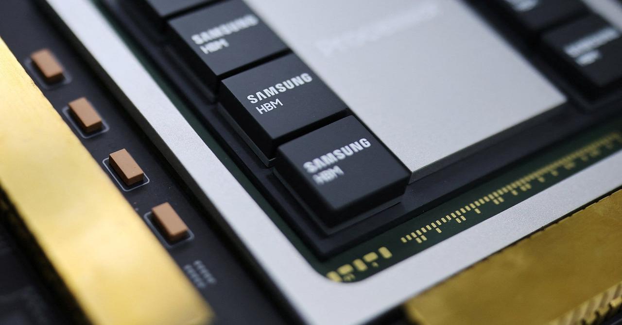
Mass production commences for HBM4 with consistent transfer speed of 11.7Gbps, capable of up to 13Gbps Leading-edge DRAM with 4nm logic base die maximizes performance, reliability and energy efficiency for next-generation datacenters Secure process technology and supply capabilities strengthen Samsung's HBM roadmap beyond HBM4 Samsung Electronics, a global leader in advanced memory technology, today announced that it has begun mass production of its industry-leading HBM4 and has shipped commercial products to customers. This achievement marks a first in the industry, securing an early leadership position in the HBM4 market. By proactively leveraging its most advanced 6th-generation 10 nanometer (nm)-class DRAM process (1c), the company achieved stable yields and industry-leading performance from the outset of mass production -- all accomplished seamlessly and without any additional redesigns. "Instead of taking the conventional path of utilizing existing proven designs, Samsung took the leap and adopted the most advanced nodes like the 1c DRAM and 4nm logic process for HBM4," said Sang Joon Hwang, Executive Vice President and Head of Memory Development at Samsung Electronics. "By leveraging our process competitiveness and design optimization, we are able to secure substantial performance headroom, enabling us to satisfy our customers' escalating demands for higher performance, when they need them." Setting the Bar for Maximum Performance and Efficiency Samsung's HBM4 delivers a consistent processing speed of 11.7 gigabits-per-second (Gbps), exceeding the industry standard of 8Gbps by approximately 46% and setting a new benchmark for HBM4 performance. This represents a 1.22x increase over the maximum pin speed of 9.6Gbps of its predecessor, HBM3E. HBM4's performance can be further enhanced up to 13Gbps, as well, effectively mitigating data bottlenecks that intensify as AI models continue to scale up. Also, total memory bandwidth per single stack is increased by 2.7x compared to HBM3E, to a maximum of 3.3 terabytes-per-second (TB/s). Through 12-layer stacking technology, Samsung offers HBM4 in capacities ranging from 24 gigabytes (GB) to 36GB. The company will also keep its capacity options aligned with future customer timelines by utilizing 16-layer stacking, which will expand offerings to up to 48GB. In order to address power consumption and thermal challenges driven by the doubling of data I/Os from 1,024 to 2,048 pins, Samsung has integrated advanced low-power design solutions into the core die. HBM4 also achieves a 40% improvement in power efficiency by leveraging low-voltage through silicon via (TSV) technology and power distribution network (PDN) optimization, while enhancing thermal resistance by 10% and heat dissipation by 30%, compared to HBM3E. By bringing outstanding performance, energy efficiency and high reliability to tomorrow's datacenter environments, Samsung's HBM4 enables customers to achieve maximized GPU throughput and effectively manage their total cost of ownership (TCO). Comprehensive Yet Agile Production Capabilities Samsung is committed to advancing its HBM roadmap through its comprehensive manufacturing resources -- including one of the largest DRAM production capacities and dedicated infrastructures in the industry -- ensuring a resilient supply chain to meet the projected surge in HBM4 demand. A tightly integrated Design Technology Co-Optimization (DTCO) between the company's Foundry and Memory Businesses allows it to secure the highest standards of quality and yield. Additionally, extensive in-house expertise in advanced packaging allows for streamlined production cycles and reduced lead times. Samsung also plans to broaden the scope of its technical partnership with key partners, based on close discussions with global GPU manufacturers and hyperscalers focused on next-generation ASIC development. Samsung anticipates that its HBM sales will more than triple in 2026 compared to 2025, and is proactively expanding its HBM4 production capacity. Following the successful introduction of HBM4 to market, sampling for HBM4E is expected to begin in the second half of 2026, while custom HBM samples will start reaching customers in 2027, according to their respective specifications.
[4]
Samsung starts mass production of next-gen AI memory chip
The high-bandwidth HBM4 chips are seen as a key component needed to scale-up the vast data centres powering the explosion in artificial intelligence. US tech giant Nvidia -- the world's most valuable company -- is widely expected to be one of Samsung's main buyers. Samsung said it had "begun mass production of its industry-leading HBM4 and has shipped commercial products to customers". "This achievement marks a first in the industry, securing an early leadership position in the HBM4 market," the South Korean company said in a statement. A global frenzy to build AI data centres has sent orders for advanced, high‑bandwidth memory microchips soaring. Samsung said its new chip was significantly faster than older models, exceeding industry standards for processing speed by more than 40 percent. This would satisfy "escalating demands for higher performance", the company said. Samsung Electronics stock was up more than six percent in afternoon trade on South Korea's stock exchange. The South Korean government has pledged to become one of the world's top three AI powers, alongside the United States and China. Samsung and its South Korean rival SK hynix are already among the leading producers of high-performance memory chips, and the two companies had raced to start HBM4 production. Taipei-based research firm TrendForce predicts that memory chip industry revenue will surge to a global peak of more than $840 billion in 2027. Samsung Electronics posted record quarterly profits earlier this year, riding on massive market demand for its powerful memory chips. The company has already earmarked billions of dollars to expand chip production facilities, pledging to continue spending in "transitioning to advanced manufacturing processes and upgrading existing production lines to meet rising demand". Nvidia designs hardware that powers AI computing, and has an almost insatiable demand for memory chips made by the likes of Samsung and SK hynix. The US-based company's almost singular role in the AI revolution has taken the world by storm since the introduction of OpenAI's ChatGPT in late 2022. Apple, Microsoft and Amazon have also developed chips with AI in mind, but for now are stuck trying to get their hands on Nvidia's coveted products. Major electronics manufacturers and industry analysts have warned that chipmakers focusing on AI sales will cause higher retail prices for consumer products across the board.
[5]
Samsung officially ships HBM4 ready for NVIDIA's next-gen Rubin AI chips
TL;DR: Samsung has officially launched its next-generation HBM4 memory, featuring up to 13Gbps transfer speeds and 3.3TB/sec bandwidth per stack, surpassing industry standards. Built on advanced 4nm and 1c DRAM processes, Samsung's HBM4 powers NVIDIA's Rubin AI chips, enhancing performance and energy efficiency for future AI applications. Samsung has been fighting hard on its semiconductor and HBM memory business over the last few years, but now it has officially started commercially deploying its next-gen HBM4 memory, ready for NVIDIA's new Rubin AI chips. The company explained in a press release that its new HBM4 memory has transfer speeds of 11.7Gbps, but when overclocked like NVIDIA needs it, Samsung's new HBM4 is capable of 13Gbps. Its new leading-edge DRAM is based on a 4nm logic die for maximum performance, fabbed in-house at Samsung Foundry, with its 1c DRAM also in play. Sang Joon Hwang, Executive Vice President and Head of Memory Development at Samsung Electronics, said: "Instead of taking the conventional path of utilizing existing proven designs, Samsung took the leap and adopted the most advanced nodes like the 1c DRAM and 4nm logic process for HBM4. By leveraging our process competitiveness and design optimization, we are able to secure substantial performance headroom, enabling us to satisfy our customers' escalating demands for higher performance, when they need them". Samsung's new HBM4 with its 11.7Gbps stock speeds exceeds the industry standard of 8Gbps by around 46% and sets a new benchmark for HBM4 performance. This is a 1.22x increase over the 9.6Gbps maximum pin speed of HBM3E, with total memory bandwidth per single stack of HBM4 being 2.7x higher than HBM3E for a total of 3.3TB/sec memory bandwidth. Samsung and NVIDIA are working together on HBM4, with Samsung explaining in its press release that with incredibly high bandwidth and energy efficiency, Samsung's advanced HBM solutions are expected to help accelerate the development of future AI applications, and form a critical foundation for manufacturing infrastructure driven by these technologies.
[6]
Samsung starts HBM4 shipments as early as third week of February
Samsung Electronics will commence mass production and shipment of its sixth-generation HBM4 high-bandwidth memory chips later this month for Nvidia graphics processing units powering the Vera Rubin AI accelerator platform, set to launch in the second half of 2026, with shipments starting as early as the week after the Lunar New Year holiday. The HBM4 chips achieve data-processing speeds of up to 11.7 gigabits per second. This performance exceeds the JEDEC industry standard of 8 gigabits per second by 37 percent. Compared to the previous HBM3E generation, the speed improvement stands at 22 percent. Memory bandwidth per stack reaches up to 3 terabytes per second. This figure amounts to roughly 2.4 times the bandwidth of the HBM3E predecessor. Samsung employs a vertically integrated manufacturing model for these chips. Unlike competitors that depend on external foundries like Taiwan Semiconductor Manufacturing Company for the base logic die, Samsung produces this component using its internal 4-nanometer foundry process. The company combines this with its 1c DRAM technology, which represents its 10-nanometer-class sixth-generation memory process. An industry source stated to the Korea JoongAng Daily, "Samsung, which has the world's largest production capacity and the broadest product lineup, has demonstrated a recovery in its technological competitiveness by becoming the first to mass-produce the highest-performing HBM4." This positions Samsung as the initial producer of these top-tier HBM4 chips on a mass scale. Samsung gains a timing edge over SK Hynix, its main competitor. SK Hynix delayed its HBM4 mass-production from February to March or April 2026. Currently dominant in the HBM market, SK Hynix plans to continue HBM3E as its primary product through at least the first half of 2026. This decision stems from adjustments in Nvidia's product strategy. Samsung completed Nvidia's quality certification process and obtained purchase orders. The company aligned its production schedule with Nvidia's plans for the Vera Rubin launch. In Nvidia's tests, Samsung's HBM4 chips earned the highest evaluation scores for operating speed and power efficiency. To address rising demand for AI memory, Samsung intends to expand HBM production capacity by about 50 percent by the end of 2026. The target reaches roughly 250,000 wafers per month, up from the current 170,000 wafers. At its Pyeongtaek Plant 4 facility, a new DRAM production line will contribute 100,000 to 120,000 additional wafers of monthly capacity. This expansion equates to an 18 percent increase in Samsung's overall DRAM production capability.
[7]
Samsung starts mass production of next-gen AI memory chip - The Economic Times
Samsung Electronics has started mass production of a next-generation memory chip to power artificial intelligence, the South Korean firm announced Thursday, touting an "industry-leading" breakthrough. The high-bandwidth "HBM4" chips are a key component for AI data centres, with US tech giant Nvidia -- now the world's most valuable company -- widely expected to be one of Samsung's main customers. Samsung said it had "begun mass production of its industry-leading HBM4 and has shipped commercial products to customers". "This achievement marks a first in the industry, securing an early leadership position in the HBM4 market," it said in a statement. A global frenzy to build AI data centres has sent orders for advanced, high‑bandwidth memory microchips soaring. South Korea's two chip giants, SK hynix and Samsung, have been racing to start HBM4 production. Taipei-based research firm TrendForce predicts that memory chip industry revenue will surge to a global peak of more than $840 billion in 2027. The South Korean government has pledged to become one of the world's top three AI powers, alongside the United States and China. Samsung and SK hynix are among the leading producers of high-performance memory chips.
[8]
Samsung Begins HBM4 Memory Mass Production With Up To 13 Gbps Speeds & 48 GB Capacities
Samsung has officially commenced mass production and shipment of its next-gen HBM4 memory with up to 13 Gbps speeds & 48 GB capacities. Samsung Commences Mass Production & Shipment of HBM4 Memory: Up To 13 Gbps Speeds, 3.3 TB/s Bandwidth Per Stack, & 48 GB Capacities In 16-Hi Stacks Press Release: Samsung Electronics, a global leader in advanced memory technology, today announced that it has begun mass production of its industry-leading HBM4 and has shipped commercial products to customers. This achievement marks a first in the industry, securing an early leadership position in the HBM4 market. By proactively leveraging its most advanced 6th-generation 10-nanometer (nm)-class DRAM process (1c), the company achieved stable yields and industry-leading performance from the outset of mass production -- all accomplished seamlessly and without any additional redesigns. Setting the Bar for Maximum Performance and Efficiency Samsung's HBM4 delivers a consistent processing speed of 11.7 gigabits-per-second (Gbps), exceeding the industry standard of 8Gbps by approximately 46% and setting a new benchmark for HBM4 performance. This represents a 1.22x increase over the maximum pin speed of 9.6Gbps of its predecessor, HBM3E. HBM4's performance can be further enhanced up to 13Gbps, as well, effectively mitigating data bottlenecks that intensify as AI models continue to scale up. Also, total memory bandwidth per single stack is increased by 2.7x compared to HBM3E, to a maximum of 3.3 terabytes-per-second (TB/s). Through 12-layer stacking technology, Samsung offers HBM4 in capacities ranging from 24 gigabytes (GB) to 36GB. The company will also keep its capacity options aligned with future customer timelines by utilizing 16-layer stacking, which will expand offerings to up to 48GB. In order to address power consumption and thermal challenges driven by the doubling of data I/Os from 1,024 to 2,048 pins, Samsung has integrated advanced low-power design solutions into the core die. HBM4 also achieves a 40% improvement in power efficiency by leveraging low-voltage through silicon via (TSV) technology and power distribution network (PDN) optimization, while enhancing thermal resistance by 10% and heat dissipation by 30%, compared to HBM3E. By bringing outstanding performance, energy efficiency, and high reliability to tomorrow's datacenter environments, Samsung's HBM4 enables customers to achieve maximized GPU throughput and effectively manage their total cost of ownership (TCO). Comprehensive Yet Agile Production Capabilities Samsung is committed to advancing its HBM roadmap through its comprehensive manufacturing resources -- including one of the largest DRAM production capacities and dedicated infrastructures in the industry -- ensuring a resilient supply chain to meet the projected surge in HBM4 demand. A tightly integrated Design Technology Co-Optimization (DTCO) between the company's Foundry and Memory Businesses allows it to secure the highest standards of quality and yield. Additionally, extensive in-house expertise in advanced packaging allows for streamlined production cycles and reduced lead times. Samsung also plans to broaden the scope of its technical partnership with key partners, based on close discussions with global GPU manufacturers and hyperscalers focused on next-generation ASIC development. Samsung anticipates that its HBM sales will more than triple in 2026 compared to 2025, and is proactively expanding its HBM4 production capacity. Following the successful introduction of HBM4 to market, sampling for HBM4E is expected to begin in the second half of 2026, while custom HBM samples will start reaching customers in 2027, according to their respective specifications. Follow Wccftech on Google to get more of our news coverage in your feeds.
[9]
Samsung HBM4 memory enters mass production
Samsung has announced that it has commenced mass production of its fourth-generation High Bandwidth Memory (HBM4) and has begun shipping commercial products to customers. The move signals an aggressive push by the South Korean tech giant to secure an early foothold in the next-generation memory market, which is critical for supporting scaling AI models. Utilizing its 6th-generation 10 nanometer (nm)-class DRAM process (known as 1c), Samsung reports that it achieved stable yields immediately upon entering mass production without requiring additional redesigns. According to specifications released by the company, the new HBM4 modules offer significant performance upgrades over the previous generation, HBM3E. Samsung states that the new memory delivers a consistent processing speed of 11.7 gigabits-per-second (Gbps), This speed exceeds the current industry standard of 8Gbps by approximately 9.6Gbps and represents a 1.22x increase over the maximum pin speed of HBM3E. The company noted that performance could potentially be enhanced up to 13Gbps to mitigate data bottlenecks associated with large-scale AI processing. In terms of bandwidth, the total memory bandwidth per single stack has increased by 2.7x compared to HBM3E, reaching a maximum of 3.3 terabytes-per-second (TB/s). Samsung is currently offering HBM4 in capacities ranging from 24GB to 36GB via 12-layer stacking technology. To align with future customer requirements, the company plans to introduce 16-layer stacking, which will expand capacity offerings up to 48GB. Addressing the physical challenges of doubling data I/Os from 1,024 to 2,048 pins, Samsung has integrated specific power and thermal management solutions: Samsung is leveraging a Design Technology Co-Optimization (DTCO) strategy, which integrates operations between its Foundry and Memory businesses, to manage quality and yield. The company is also utilizing in-house advanced packaging facilities to streamline production cycles. Looking forward, Samsung projects that its HBM sales will more than triple in 2026 compared to 2025 figures. The company has outlined the following timeline for future iterations: The company indicated it plans to broaden technical partnerships with global GPU manufacturers and hyperscalers, specifically focusing on next-generation ASIC development. Regarding this, Sang Joon Hwang, Executive Vice President and Head of Memory Development at Samsung Electronics, said:
[10]
Samsung Electronics begins HBM4 shipping for 1st time - The Korea Times
Samsung Electronics announced Thursday that it has begun mass production and shipping of high-bandwidth memory 4 (HBM4), marking the world's first delivery of the advanced chip for artificial intelligence (AI) accelerators to customers. For over a year, the company's chipmaking Device Solutions division had refrained from officially announcing updates related to its HBM, as its predecessor HBM3E struggled in the market due to yield issues. With the latest announcement, Samsung appears to be signaling confidence in its technological advantages and stability in the mass production system. Samsung Electronics' HBM4 chips are using its 1c process, the sixth-generation 10-nanometer-class DRAM technology, for the DRAM cell die, while using a 4-nanometer foundry process for the base die. While its main rival SK hynix is using a previous-generation 1b process for HBM4 to focus on stability, Samsung said it has pursued a more advanced process from the designing phase to secure top-tier performance, and achieved stable yields without any redesigns. "Instead of taking the conventional path of using existing proven designs, Samsung took the leap and adopted the most advanced nodes like the 1c DRAM and 4-nanometer logic process for HBM4," said Hwang Sang-joon, head of memory development at Samsung Electronics. "By leveraging our process competitiveness and design optimization, we are able to secure substantial performance headroom, enabling us to satisfy our customers' escalating demands for higher performance, when they need it." Based on these technologies, Samsung had its HBM4 chips achieve data processing speeds of up to 11.7 gigabits per second (Gbps), exceeding the Joint Electron Device Engineering Council's standard of 8 Gbps. This represents a 1.22-fold increase over the maximum pin speed of 9.6 Gbps of HBM3E. The company said its HBM4 performance can be further enhanced up to 13Gbps, effectively mitigating data bottlenecks stemming from scaling AI models. The total memory bandwidth per single stack is increased by 2.7 times compared to HBM3E, to a maximum of 3.3 terabytes per second. Samsung said its HBM4 chips are based on 12-layer stacking technology, offering capacities ranging from 24 gigabytes to 36 gigabytes. Each single stack provides 3 gigabytes of capacity. The company added that it will also keep its capacity options aligned with future customer timelines by using 16-layer stacking technology, meaning the capacity could grow up to 48 gigabytes. To improve power efficiency, Samsung has integrated advanced low-power design solutions into the core die. HBM4 achieves a 40 percent improvement in power efficiency, 10 percent in thermal resistance and 30 percent in heat dissipation, compared to HBM3E. It also said the company plans to roll out samples of HBM4E in the second half of this year and begin shipping custom HBM samples meeting specific customer requirements in 2027. Samsung said that its HBM revenue for this year is expected to triple from that of 2025, and the company is preemptively expanding its HBM4 production capacity. For this, the company plans to use the P5 plant of its Pyeongtaek campus in Gyeonggi Province as the core production base when it begins full-scale operations in 2028.
[11]
Samsung shows confidence in HBM, portrays next-gen road map - The Korea Times
Samsung Electronics Chief Technology Officer Song Jai-hyuk speaks during his keynote speech for SEMICON Korea 2026 at Coex in Seoul, Wednesday. Yonhap Samsung Electronics Chief Technology Officer Song Jai-hyuk said Wednesday the company's high-bandwidth memory 4 (HBM4) chip is showing "good" manufacturing yield, adding that clients have expressed strong satisfaction with its performance. "We may have fallen short of demonstrating our world-class technological responsiveness to customer needs for a while, but this should be seen as a return to that standard," Song told reporters before his keynote speech for SEMICON Korea 2026 in Seoul. Samsung reportedly plans to begin HBM4 mass production and shipping to major customers later this month. Its HBM4 chips are using its 1c process, the sixth-generation 10-nanometer-class DRAM technology, for the DRAM cell die, while using a 4-nanometer foundry process for the base die. Based on these technologies, Samsung had its HBM4 chips achieve data processing speeds of up to 11.7 gigabits per second (Gbps), exceeding the Joint Electron Device Engineering Council's standard of 8 Gbps. Since they are the industry's latest technologies, questions have been raised over how the company will secure production yield as operations ramp up, but Song expressed confidence. "It is difficult to describe (the yield) in numbers, but I can say the status is very good," he said, adding that customers are "very satisfied" with the performance of the chip. "In terms of technology, we believe we remain at the top. The question of how we manage our portfolio falls into the realm of business ... We believe our in-house capabilities spanning memory, foundry and packaging create the best environment for making artificial intelligence (AI)-driven products, and the combination is generating synergy." During his keynote speech, Song stressed Samsung Electronics' advantage as a company capable of foundry, memory and chip packaging businesses, saying it will demonstrate a "distinctive and powerful Samsung-only semiconductor synergy through co-optimization." To cope with growing workloads required for AI accelerators, Song said Samsung is considering custom HBM based on a compute-in-base-die architecture, which allows part of the workload typically handled by graphics processing units and other logic chips to be processed by the memory's base die. Through this approach, he predicted power efficiency could be improved by up to 2.8 times. He also introduced a technology dubbed zHBM, in which HBM is stacked vertically on top of logic chips, saying it could deliver another major leap in bandwidth and power efficiency. Under this architecture, bandwidth is expected to increase fourfold, while power consumption could be reduced to one-quarter of current levels. SK hynix Senior Vice President Lee Sung-hoon also shared the outlook that the semiconductor industry will face unprecedented technological challenges for the next 10 years, and that the industry can find a breakthrough through AI-driven research and data collaboration across the chip ecosystem. SEMICON Korea, the country's largest semiconductor industry fair, kicked off its three-day run at Coex in southern Seoul the same day. This year's edition is the largest of its kind, with more than 550 companies in the semiconductor value chain participating, including Nvidia, Samsung Electronics, SK hynix, Intel, Kioxia, Micron, ASML and Applied Materials. More than 75,000 people have signed up to attend the event, according to SEMI Korea. Under the theme of Transform Tomorrow, the event will feature more than 30 sessions where over 200 experts and other speakers will discuss advanced manufacturing technologies, AI, market trends and other key topics in the industry.
[12]
Samsung begins shipments of HMB4 chips for AI; sees sales tripling in 2026 By Investing.com
Investing.com-- Samsung Electronics said on Thursday it had commenced mass production of advanced high-bandwidth memory chips used in artificial intelligence processors, and had shipped commercial products to customers. The electronics conglomerate said it expects its HBM chip sales to more than triple in 2026 from 2025, and that it was "proactively expanding" its HBM4 production capacity. Get more breaking news on major AI and chipmaking stocks by subscribing to InvestingPro Samsung said it had begun mass production of the fourth generation of HBM chips, HBM4, with the company claiming that its chips set a new industry benchmark for HBM4 performance and power efficiency. The South Korean memory chip giant's shares rallied over 6% to a record high on Thursday. It also said it is the first company to mass-produce and ship the HBM4 chips. Samsung's announcement comes shortly after U.S. rival Micron Technology Inc (NASDAQ:MU) said it had commenced shipments of HMB4 chips. The two appear to have beaten rival SK Hynix Inc (KS:000660) in commencing shipments of HBM4 memory. The company said it will begin sampling for HBM4E- an advanced version of the chips- in the second half of 2026. Samsung's announcement on Thursday was largely telegraphed by a slew of media reports over the past month. The company is reportedly a major memory supplier to NVIDIA Corporation (NASDAQ:NVDA), and will supply chips for Nvidia's next-gen Vera Rubin AI processors. HBM are a class of memory chips crucial towards AI development, given the large computing requirements of generative AI models. They facilitate much faster processing speeds and memory capacity. Samsung has also largely shifted focus towards more high-margin HBM and AI memory products in recent quarters, amid outsized demand from the industry.
[13]
Imperative to stay ahead in memory chips - The Korea Times
Samsung Electronics building in Seocho District, Seoul, Jan. 28. The Korean tech giant has said it will begin shipping sixth-generation high-bandwidth memory in the third week of February to power Nvidia's Vera Rubin. Korean tech giant Samsung has finally announced that it will start mass-producing sixth-generation high-bandwidth memory (HBM4) chips after the Lunar New Year holiday next week. For the company and its investors, the awaited news somewhat alleviates concerns about the company's competitiveness in the HBM sector, especially as the semiconductor sector makes up for one-fifth of the nation's exports and as Samsung Electronics and SK hynix together buttressed the recent hike in the Korean bourse. Samsung's plan to ship starting next week to power Nvidia's Vera Rubin AI accelerator, combined with SK hynix's top-notch performance in the high-bandwidth chips, paints a positive outlook for Korean semiconductors. At least until we begin to take a broader view and look at the global market. As the firms and nations accelerate their artificial intelligence revolution, the pressing global demand for chips has prompted some overseas firms such as Dell and Intel to source Chinese memory chips over Korean ones. Supported by a massive state-led fund and policies, Chinese memory chip manufacturers have been making leaps and bounds. One of its top memory manufacturers, ChangXin Memory Technologies (CXMT), announced that it has begun mass production of HBM3, the 4th-generation HBM. Experts in Korea are closely watching the gap in technology advancement between the two countries. When Korea began mass-producing HBM3 in 2023, it was estimated that it would take three years for Chinese firms to catch up. The three-year gap, most experts noted, is narrowing, considering that before HBM3, it was assumed that Chinese memory firms would need four years to reach that level. One could arguably assess that with its dominance in the memory sector and recent advancement in HBM4, the Korean sector enjoys an overwhelming lead. It is true that Korea's Samsung and SK hynix, together with U.S.-based Micron Technology, account for 90 percent of the dynamic random access memory (DRAM) market share, according to many industry reports. But the same industry assessment papers also point out that an acceleration in China's catch-up speed in top memory technology will be a possible risk factor to watch out for. Meanwhile, Korean firms need to focus on advancing their own cutting-edge technologies through investing in research and development. Korean policymakers and legislators must keep in mind that semiconductors form a vital loop in ensuring that a nation and firms have a stable supply chain, and work to support the businesses in ensuring technological advancements. As one way to do that, policymakers and legislators should refer to the growth in China's tech-driven Fourth Industrial Revolution. The country's state support in that achievement remains incomparable, as its government-led Integrated Circuit Industry Investment Fund is regarded as the world's largest program subsidizing the semiconductor sector. China also produces a larger volume of engineering graduates than Korea. A special bill that details support for the semiconductor sector just passed muster through the ruling Democratic Party of Korea-dominated National Assembly on Jan. 29. The bill, despite intentions to expand infrastructure support for semiconductor plants such as electricity lines and water, has kept the rigid 52-hour workweek limit intact despite calls from the industry for more labor flexibility. Direct support has been reduced as well. The bill inadvertently lays pressure on existing semiconductor clusters already active with its clauses to grant larger volume of support in terms of building infrastructure, and for tax relief to those that newly set up in regions farther from the capital. It's better late than never. The political mindset prevalent in the Assembly should make room to accommodate for a cold, rational perspective regarding the political economy facing Korea.
[14]
Samsung Begins Shipments of HBM4 Products
Samsung Electronics has begun shipments of the most advanced high-bandwidth memory products, known as HBM4. The South Korean technology giant said Thursday that it is the world's first to mass produce and ship the industry's highest-performance HBM4 products. The company is looking to dominate the HBM4 market after lagging behind its rivals in recent quarters. Samsung didn't identify the clients buying its HBM4 products, which are a crucial component of artificial-intelligence chips. The world's largest memory-chip maker counts SK Hynix and Micron Technology as its closest competitors and has been seeking to become a major HBM4 supplier for Nvidia. SK Hynix has said it completed its development of HBM4 products and is preparing to ship the advanced chips. The home-country rival of Samsung has dominated the market for previous HBM versions. The development comes as the global AI chip market continues to grow rapidly, forcing HBM suppliers to keep pace. Samsung said it expects revenue from its HBM business to more than triple in 2026, and is preemptively expanding its HBM4 production. It said it is also preparing to ship an upgraded HBM4 sample product, HBM4E, in the second half of the year.
[15]
Samsung starts mass production of next-gen AI memory chip - VnExpress International
The high-bandwidth HBM4 chips are seen as a key component needed to scale-up the vast data centers powering the explosion in artificial intelligence. U.S. tech giant Nvidia -- the world's most valuable company -- is widely expected to be one of Samsung's main buyers. Samsung said it had "begun mass production of its industry-leading HBM4 and has shipped commercial products to customers". "This achievement marks a first in the industry, securing an early leadership position in the HBM4 market," the South Korean company said in a statement. A global frenzy to build AI data centers has sent orders for advanced, high‑bandwidth memory microchips soaring. Samsung said its new chip was significantly faster than older models, exceeding industry standards for processing speed by more than 40%. This would satisfy "escalating demands for higher performance", the company said. Samsung Electronics stock was up more than 6% in afternoon trade on South Korea's stock exchange. The South Korean government has pledged to become one of the world's top three AI powers, alongside the United States and China. Samsung and its South Korean rival SK hynix are already among the leading producers of high-performance memory chips, and the two companies had raced to start HBM4 production. Taipei-based research firm TrendForce predicts that memory chip industry revenue will surge to a global peak of more than $840 billion in 2027. Frontrunner Samsung Electronics posted record quarterly profits earlier this year, riding on massive market demand for its powerful memory chips. The company has already earmarked billions of dollars to expand chip production facilities, pledging to continue spending in "transitioning to advanced manufacturing processes and upgrading existing production lines to meet rising demand". An industry observer said the move would help Samsung seize the moment in the intensifying race for chips critical to AI infrastructure. "Samsung struggled in the race for HBM3 chips, lagging behind its rival SK hynix," Kim Dae-jong, a professor of business at Sejong University, told AFP. "But with the early production of HBM4, it has positioned itself as a frontrunner in the competition," he added. Nvidia designs hardware that powers AI computing, and has an almost insatiable demand for memory chips made by the likes of Samsung and SK hynix. The U.S.-based company's almost singular role in the AI revolution has taken the world by storm since the introduction of OpenAI's ChatGPT in late 2022. Apple, Microsoft and Amazon have also developed chips with AI in mind, but for now are stuck trying to get their hands on Nvidia's coveted products. Major electronics manufacturers and industry analysts have warned that chipmakers focusing on AI sales will cause higher retail prices for consumer products across the board.
Share
Share
Copy Link
Samsung and Micron have started mass production and shipping of HBM4 memory, the next-generation high-bandwidth memory critical for AI acceleration hardware. Samsung claims industry-first status with 11.7Gbps speeds and up to 3.3TB/s bandwidth, while Micron confirms it delivered product a quarter ahead of schedule. The development signals readiness for Nvidia's upcoming Vera Rubin accelerators launching in Q2 2026.
Samsung Claims First-Mover Advantage in HBM4 Production
Samsung has announced it has begun mass production of HBM4 and shipped commercial products to customers, claiming industry-first status in the high-bandwidth memory market
3
. The Korean giant's new AI memory chip delivers a consistent processing speed of 11.7 gigabits-per-second, exceeding the industry standard of 8Gbps by approximately 46%3
. Under certain conditions, users can push that transfer speed to hit 13Gbps, addressing data bottlenecks as AI models continue scaling up1
. Total memory bandwidth can reach 3.3 terabytes-per-second in a single stack, representing a 2.7x increase over HBM3E3
.
Source: Korea Times
The company leveraged its most advanced 6th-generation 10 nanometer-class DRAM process (1c) and a 4nm logic process to achieve stable yields and industry-leading performance from the outset of mass production
3
. Samsung's stock rose more than six percent following the announcement, reflecting investor confidence in the company's position within the AI semiconductor market4
.Micron Counters With Early HBM4 Delivery
Just a day before Samsung's announcement, Micron revealed it has also started high-volume HBM4 production and shipped units to customers. Speaking at a Wolfe Research event, Micron CFO Mark Murphy addressed what he called "inaccurate reporting" about the company's HBM4 position, confirming that Micron delivered product a quarter earlier than previously forecast
1
. Murphy emphasized that "our HBM yield is on track. Our HBM4 yield is on track. Our HBM4 product delivers over 11 gigabits per second speeds"1
.Micron has pre-sold every single HBM4 chip it can manufacture this year, underscoring the intense demand for AI acceleration hardware
1
. Investors responded enthusiastically, with Micron's share price spiking almost ten percent on news of its early production1
. The dual announcements leave SK Hynix as the only major memory-maker yet to confirm HBM4 production has started1
.Critical Enabler for Nvidia's Vera Rubin Launch
The timing of these HBM4 shipments matters significantly for Nvidia, which plans to release its Vera Rubin accelerators in the second quarter of 2026 using memory from Samsung and SK Hynix
1
. Samsung and Nvidia are working closely together on HBM4, with the advanced memory solutions expected to help accelerate the development of future AI applications and form a critical foundation for manufacturing infrastructure driven by AI computing technologies5
. The unnamed customer Samsung has shipped to is likely Nvidia, which has confirmed its forthcoming Nvidia Rubin AI chips will use the memory1
.
Source: Wccftech
Samsung's HBM4 represents a 1.22x increase over the maximum pin speed of 9.6Gbps of HBM3E, positioning it to satisfy escalating demands for higher performance in next-generation datacenters
3
. Sang Joon Hwang, Executive Vice President and Head of Memory Development at Samsung Electronics, explained that "instead of taking the conventional path of utilizing existing proven designs, Samsung took the leap and adopted the most advanced nodes"3
.Related Stories
Energy Efficiency and Thermal Management Advances
To address power consumption and thermal challenges driven by the doubling of data I/Os from 1,024 to 2,048 pins, Samsung integrated advanced low-power design solutions into the core die
3
. HBM4 achieves a 40% improvement in energy efficiency by leveraging low-voltage through silicon via (TSV) technology and power distribution network optimization, while enhancing thermal resistance by 10% and heat dissipation by 30% compared to HBM3E1
. These improvements mean the memory uses less electricity and runs cooler, suggesting users can look forward to slower growth in their energy bills1
.
Source: France 24
Production Capacity and Market Outlook
Through 12-layer stacking technology, Samsung offers HBM4 in capacities ranging from 24 gigabytes to 36GB, with plans to expand offerings to up to 48GB using 16-layer stacking
3
. Samsung anticipates that its HBM sales will more than triple in 2026 compared to 2025, and is proactively expanding its production capacity3
. The company expects to ship samples of HBM4E in the second half of 2026, while custom HBM samples will start reaching customers in 20271
.Taipei-based research firm TrendForce predicts that memory chip industry revenue will surge to a global peak of more than $840 billion in 2027
4
. However, the shift in production capacity to high-margin products for AI applications may bring price rises for consumer memory, as Samsung and others focus on serving hyperscalers and AI data centers1
. Major electronics manufacturers and industry analysts have warned that chipmakers focusing on AI sales will cause higher retail prices for consumer products across the board4
. Samsung's comprehensive manufacturing resources and tightly integrated Design Technology Co-Optimization between its Foundry and Memory Businesses allow it to secure the highest standards of quality and yield while ensuring a resilient supply chain3
.References
Summarized by
Navi
[1]
Related Stories
Samsung HBM4 nears Nvidia approval as rivalry with SK Hynix intensifies for Rubin AI platform
26 Jan 2026•Technology
Samsung gains ground in HBM4 race as Nvidia production ignites AI memory battle with SK Hynix, Micron
02 Jan 2026•Technology
SK hynix Leads the Charge in Next-Gen AI Memory with World's First 12-Layer HBM4 Samples
19 Mar 2025•Technology

Recent Highlights
1
OpenAI shuts down Sora video app after six months, ending Disney's $1 billion investment deal
Technology

2
AI-Generated Val Kilmer to Posthumously Appear in As Deep as the Grave After His Death
Entertainment and Society

3
Supermicro Co-Founder Indicted in $2.5 Billion Nvidia AI Chip Smuggling Scheme to China
Policy and Regulation
Recent Highlights
Today's Top Stories


Your Daily Dose of Curated AI News
Don’t drown in AI news. We cut through the noise - filtering, ranking and summarizing the most important AI news, breakthroughs and research daily. Spend less time searching for the latest in AI and get straight to action.