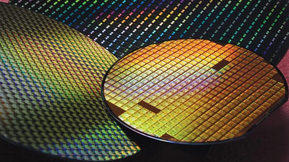
TSMC and Cadence Partner to Advance AI-Driven Chip Design and 3D IC Solutions
2 Sources
2 Sources
[1]
TSMC and Cadence Collaborate to Deliver AI-Driven Advanced-Node Design Flows, Silicon-Proven IP and 3D-IC Solutions
SAN JOSE, Calif.-(BUSINESS WIRE)-September 25, 2024- Cadence Design Systems, Inc. (Nasdaq: CDNS) today announced that it is collaborating with TSMC to enhance productivity and optimize product performance for AI-driven advanced-node designs and 3D-ICs. The rapid adoption of AI applications has created unprecedented demand for advanced silicon solutions capable of handling colossal datasets and computations. To meet these escalating requirements, the industry is pushing the boundaries of advanced-node silicon and 3D-IC technologies. TSMC and Cadence are at the forefront of this revolution, together empowering customers to accelerate time to market while increasing performance. This press release features multimedia. View the full release here: https://www.businesswire.com/news/home/20240925780123/en/ TSMC has certified Cadence's industry-leading digital and custom design flows for implementation and signoff on TSMC's latest N3 and N2P process technologies. As long-standing design technology co-optimization (DTCO) partners, TSMC and Cadence continue that tradition by collaborating to optimize power, performance and area (PPA) on A16, adding EDA features to enable advanced features such as backside routing. Cadence and TSMC are also collaborating on Cadence.AI to drive next-generation digital and analog design automation fueled by AI, delivering industry-leading productivity and quality of results. Cadence.AI is a chips-to-systems AI platform spanning all aspects of design and verification. The collaboration between TSMC and Cadence is focused on three main domains: The Cadence Integrity 3D-IC Platform is a leading system-level exploration solution and a single-vendor platform that unifies packaging, analog and digital implementation-making efficient 3D-IC design possible. This opens new opportunities for innovation by supporting all the latest 3Dblox features and constructs. To enable the ultra-high-density interconnect in TSMC 3DFabric technologies, TSMC and Cadence are collaborating on a next-generation high-capacity substrate router for die-to-die and die-to-substrate connections. Multiphysics analyses and optimization is a critical dimension of success for 3D-IC technologies. TSMC and Cadence are collaborating to enable warpage/stress analysis for TSMC 3DFabric in addition to electrical/thermal analysis, and Cadence's Celsius Studio warpage/stress analysis simulation results have been validated. Thermal and voltage impacts on power/IR/STA are also enabled and verified inside the Cadence Integrity 3D-IC Platform for TSMC 3DFabric. The AI factories' insatiable appetite for data is increasing the requirements for interconnects and pushing power envelopes. Cadence has a broad portfolio of critical IP for efficiently moving data between chiplets and across data centers, including Universal Chiplet Interconnect Express (UCIe) 1.0, PCI Express (PCIe) 6.0 and the world's first silicon-proven GDDR7 on TSMC N3, running at 32Gbps, which provides the best price/performance for AI interfaces in both data centers and network edges. To address the growing communication challenges between these chips, Cadence silicon photonics design enablement solutions support TSMC's Compact Universal Photonic Engine (COUPE). TSMC and Cadence are jointly collaborating with the leaders in the automotive space. As the silicon content in today's automotive designs continues to grow, IP development for current and future process nodes, such as TSMC N5A and later N3A, is even more critical. TSMC and Cadence have also collaborated to showcase the accuracy and scalability offered by Cadence's front-to-backend chip design flows on the Cloud for TSMC's advanced process nodes. Through this collaboration, mutual customers can shorten design schedules by adopting Cadence's wide range of Cloud solutions. "TSMC and Cadence have a long-standing, successful partnership that turns the world's designs into silicon reality," said Chin-Chi Teng, senior vice president and general manager of the Digital & Signoff Group at Cadence. "Together, we are revolutionizing the future of silicon design with AI-powered EDA software, enabled for TSMC's latest process technologies. Our ongoing collaboration on innovative solutions for next-generation technologies like TSMC A16 and 3Dblox is paving the way for the AI factories of tomorrow." "In collaboration with Cadence, we've successfully enabled AI-optimized design flows for TSMC's N2 technology and are driving advancements in 3D-IC design," said Dan Kochpatcharin, head of Ecosystem and Alliance Management Division at TSMC. "This marks a significant leap forward in digital and custom solutions, paving the way for the technology innovations that will power the AI infrastructure." About Cadence Cadence is a pivotal leader in electronic systems design, building upon more than 30 years of computational software expertise. The company applies its underlying Intelligent System Design strategy to deliver software, hardware and IP that turn design concepts into reality. Cadence customers are the world's most innovative companies, delivering extraordinary electronic products from chips to boards to complete systems for the most dynamic market applications, including hyperscale computing, 5G communications, automotive, mobile, aerospace, consumer, industrial and healthcare. For 10 years in a row, Fortune magazine has named Cadence one of the 100 Best Companies to Work For. Learn more at cadence.com. © 2024 Cadence Design Systems, Inc. All rights reserved worldwide. Cadence, the Cadence logo and the other Cadence marks found at www.cadence.com/go/trademarks are trademarks or registered trademarks of Cadence Design Systems, Inc. UCIe Consortium, Universal Chiplet Interconnect Express and UCIe are trademarks of the UCIe Consortium. PCI Express and PCIe are registered trademarks of PCI-SIG. All other trademarks are the property of their respective owners. Category: Featured View source version on businesswire.com: https://www.businesswire.com/news/home/20240925780123/en/
[2]
TSMC and Cadence Collaborate to Deliver AI-Driven Advanced-Node Design Flows, Silicon-Proven IP and 3D-IC Solutions By Investing.com
SAN JOSE, Calif.--(BUSINESS WIRE)--Cadence Design Systems, Inc. (Nasdaq: CDNS) today announced that it is collaborating with TSMC to enhance productivity and optimize product performance for AI-driven advanced-node designs and 3D-ICs. The rapid adoption of AI applications has created unprecedented demand for advanced silicon solutions capable of handling colossal datasets and computations. To meet these escalating requirements, the industry is pushing the boundaries of advanced-node silicon and 3D-IC technologies. TSMC and Cadence are at the forefront of this revolution, together empowering customers to accelerate time to market while increasing performance. This press release features multimedia. View the full release here: https://www.businesswire.com/news/home/20240925780123/en/ TSMC has certified Cadence's industry-leading digital and custom design flows for implementation and signoff on TSMC's latest N3 and N2P process technologies. As long-standing design technology co-optimization (DTCO) partners, TSMC and Cadence continue that tradition by collaborating to optimize power, performance and area (PPA) on A16, adding EDA features to enable advanced features such as backside routing. Cadence and TSMC are also collaborating on Cadence.AI to drive next-generation digital and analog design automation fueled by AI, delivering industry-leading productivity and quality of results. Cadence.AI is a chips-to-systems AI platform spanning all aspects of design and verification. The collaboration between TSMC and Cadence is focused on three main domains: The Cadence Integrity™ 3D-IC Platform is a leading system-level exploration solution and a single-vendor platform that unifies packaging, analog and digital implementation"making efficient 3D-IC design possible. This opens new opportunities for innovation by supporting all the latest 3Dblox features and constructs. To enable the ultra-high-density interconnect in TSMC 3DFabric™ technologies, TSMC and Cadence are collaborating on a next-generation high-capacity substrate router for die-to-die and die-to-substrate connections. Multiphysics analyses and optimization is a critical dimension of success for 3D-IC technologies. TSMC and Cadence are collaborating to enable warpage/stress analysis for TSMC 3DFabric in addition to electrical/thermal analysis, and Cadence's Celsius™ Studio warpage/stress analysis simulation results have been validated. Thermal and voltage impacts on power/IR/STA are also enabled and verified inside the Cadence Integrity 3D-IC Platform for TSMC 3DFabric. The AI factories' insatiable appetite for data is increasing the requirements for interconnects and pushing power envelopes. Cadence has a broad portfolio of critical IP for efficiently moving data between chiplets and across data centers, including Universal Chiplet Interconnect Express™ (UCIe™) 1.0, PCI Express ® (PCIe ®) 6.0 and the world's first silicon-proven GDDR7 on TSMC N3, running at 32Gbps, which provides the best price/performance for AI interfaces in both data centers and network edges. To address the growing communication challenges between these chips, Cadence silicon photonics design enablement solutions support TSMC's Compact Universal Photonic Engine (COUPE). TSMC and Cadence are jointly collaborating with the leaders in the automotive space. As the silicon content in today's automotive designs continues to grow, IP development for current and future process nodes, such as TSMC N5A and later N3A, is even more critical. TSMC and Cadence have also collaborated to showcase the accuracy and scalability offered by Cadence's front-to-backend chip design flows on the Cloud for TSMC's advanced process nodes. Through this collaboration, mutual customers can shorten design schedules by adopting Cadence's wide range of Cloud solutions. TSMC and Cadence have a long-standing, successful partnership that turns the world's designs into silicon reality, said Chin-Chi Teng, senior vice president and general manager of the Digital & Signoff Group at Cadence. Together, we are revolutionizing the future of silicon design with AI-powered EDA software, enabled for TSMC's latest process technologies. Our ongoing collaboration on innovative solutions for next-generation technologies like TSMC A16 and 3Dblox is paving the way for the AI factories of tomorrow. In collaboration with Cadence, we've successfully enabled AI-optimized design flows for TSMC's N2 technology and are driving advancements in 3D-IC design, said Dan Kochpatcharin, head of Ecosystem and Alliance Management Division at TSMC. This marks a significant leap forward in digital and custom solutions, paving the way for the technology innovations that will power the AI infrastructure. About Cadence Cadence is a pivotal leader in electronic systems design, building upon more than 30 years of computational software expertise. The company applies its underlying Intelligent System Design strategy to deliver software, hardware and IP that turn design concepts into reality. Cadence customers are the world's most innovative companies, delivering extraordinary electronic products from chips to boards to complete systems for the most dynamic market applications, including hyperscale computing, 5G communications, automotive, mobile, aerospace, consumer, industrial and healthcare. For 10 years in a row, Fortune magazine has named Cadence one of the 100 Best Companies to Work For. Learn more at cadence.com. © 2024 Cadence Design (NASDAQ:CDNS) Systems, Inc. All rights reserved worldwide. Cadence, the Cadence logo and the other Cadence marks found at www.cadence.com/go/trademarks are trademarks or registered trademarks of Cadence Design Systems, Inc. UCIe Consortium, Universal Chiplet Interconnect Express and UCIe are trademarks of the UCIe Consortium. PCI Express and PCIe are registered trademarks of PCI-SIG. All other trademarks are the property of their respective owners.
Share
Share
Copy Link
TSMC and Cadence announce collaboration to develop AI-driven design flows, silicon-proven IP, and 3D IC solutions for advanced semiconductor manufacturing processes, aiming to accelerate chip development and improve performance.

Collaboration Announcement
Taiwan Semiconductor Manufacturing Company (TSMC) and Cadence Design Systems have announced a strategic collaboration to develop cutting-edge solutions for the semiconductor industry. The partnership aims to deliver AI-driven advanced node design flows, silicon-proven intellectual property (IP), and three-dimensional integrated circuit (3D IC) solutions
1
.AI-Driven Design Flows
The collaboration focuses on leveraging artificial intelligence to enhance chip design processes. TSMC and Cadence are working together to develop AI-driven design flows that will support TSMC's advanced process technologies, including the N3 and N2 nodes. These innovative flows are expected to significantly improve design efficiency and accelerate time-to-market for complex chip designs
2
.Silicon-Proven IP
As part of the collaboration, Cadence will develop and deliver silicon-proven IP optimized for TSMC's advanced process technologies. This includes a wide range of IP blocks essential for modern chip designs, such as high-speed SerDes, memory interfaces, and analog/mixed-signal IP. The silicon-proven nature of these IP blocks will help reduce risk and improve reliability for chip designers using TSMC's manufacturing processes
1
.3D IC Solutions
The partnership also extends to the development of advanced 3D IC solutions. TSMC and Cadence are collaborating on tools and methodologies to support the design and manufacturing of complex 3D IC architectures. These solutions will enable chip designers to create more integrated and power-efficient designs by stacking multiple dies vertically
2
.Related Stories

Industry Impact
This collaboration between TSMC, the world's largest dedicated semiconductor foundry, and Cadence, a leading provider of electronic design automation (EDA) software, is expected to have a significant impact on the semiconductor industry. By combining TSMC's advanced manufacturing capabilities with Cadence's expertise in chip design tools and methodologies, the partnership aims to address the increasing complexity of modern chip designs and the challenges of scaling to more advanced process nodes
1
.Future Outlook
The collaboration between TSMC and Cadence is set to play a crucial role in shaping the future of semiconductor design and manufacturing. As the industry continues to push the boundaries of Moore's Law, the AI-driven design flows, silicon-proven IP, and 3D IC solutions developed through this partnership will be instrumental in enabling the next generation of high-performance, energy-efficient chips for applications ranging from mobile devices to data centers and artificial intelligence systems
2
.References
Summarized by
Navi
[1]
Related Stories
Synopsys and TSMC Collaborate to Advance AI Chip Design with Cutting-Edge Solutions
26 Sept 2024

Cadence and NVIDIA Expand Partnership to Accelerate AI-Driven Engineering and Scientific Innovation
20 Mar 2025•Technology

Cadence embeds AI across chip design tools to tackle trillion-transistor complexity by 2030
10 Feb 2026•Technology
Recent Highlights
1
Tennessee Teens Sue Elon Musk's xAI Over Grok AI-Generated Child Abuse Images
Policy and Regulation

2
Supermicro Co-Founder Indicted in $2.5 Billion Nvidia AI Chip Smuggling Scheme to China
Policy and Regulation
3
Val Kilmer to appear posthumously in As Deep as the Grave through AI-generated performance
Entertainment and Society

Recent Highlights
Today's Top Stories


Your Daily Dose of Curated AI News
Don’t drown in AI news. We cut through the noise - filtering, ranking and summarizing the most important AI news, breakthroughs and research daily. Spend less time searching for the latest in AI and get straight to action.