Gauss Labs Unveils AI-Powered Virtual Metrology Solution Panoptes VM 2.0
2 Sources
2 Sources
[1]
Gauss Labs Releases AI-Based Virtual Metrology Solution, Panoptes VM 2.0 By Investing.com
, /PRNewswire/ -- Gauss Labs announced today that it released the second version of its AI-based virtual metrology solution, Panoptes VM 2.0. Metrology: a process of measuring the physical and electrical characteristics to ensure that requirements are met in the manufacturing process Panoptes VM provides all-wafer measurement data in real-time by predicting process outcomes from sensor data. By applying this solution, it is possible to predict the process results of all products without physical full-scale measurement, significantly reducing time and resources. Gauss Labs said that Panoptes VM 2.0 is making a new leap forward with new modeling features including the Multi-Step Modeling, Operation-Group Modeling and Automatic Model Selection. With these new features, the prediction accuracy and usability have been greatly improved, compared to the previous version. Gauss Labs, an industrial AI company invested by SK hynix, first launched Panoptes VM 1.0 in . The system has been deployed to the thin film deposition process at SK hynix's high-volume manufacturing fabs since . By integrating the virtual measurement results from Panoptes VM with APC, SK hynix improved process variability by approximately 29% and also enhanced yield rate. Thin film deposition: the process of creating and depositing thin film coatings onto a substrate material APC(Advanced Process Control): a solution that adjusts process condition for equipment adaptively during a manufacturing process Variability: the scale of the quality variation of the products from a certain process. It is important to maintain a low process variability in order to keep the product quality consistent. SK hynix plans to expand the application to APC use case. With the new Multi-Step Modeling feature, it expects to cover the etching process effectively. This new feature creates prediction models using data from not only the current step but also previous steps to improve the accuracy of VM predictions which is especially critical for etching process. Etching: the process of removing unnecessary parts on the exterior of the circuit engraved on the wafer through photolithography Panoptes VM 2.0 also provides the Operation-Group Modeling that allows the users to group data from similar operations for more effective modeling even when the data is scarce and the Automatic Model Selection, which supports multi-algorithm architecture and automatically selects the best performing model based on data characteristics to further improve the accuracy of VM as well as usability. Gauss Labs, headquartered in , was founded in 2020 with the vision of "revolutionizing manufacturing with AI" and has focused on "developing AI solutions for manufacturing data intelligence (MDI)." , Chief Executive Officer of Gauss Labs, said, "Our concerted efforts over the past 4 years are now creating meaningful impact in the semiconductor industry, the most advanced manufacturing sector. Equipped with our state-of-the-art industrial AI technology, we will continue our march towards the global industrial AI market." MDI(Manufacturing Data Intelligence): extracting valuable information and insights from a vast amount of raw manufacturing data that cannot be easily analyzed by humans About SK hynix Inc. (KS:000660) SK hynix Inc., headquartered in , is the world's top tier semiconductor supplier offering Dynamic Random Access Memory chips ("DRAM"), flash memory chips ("NAND flash") and CMOS Image Sensors ("CIS") for a wide range of distinguished customers globally. The Company's shares are traded on the Korea Exchange, and the Global Depository shares are listed on the Luxemburg Stock Exchange. Further information about SK hynix is available at www.skhynix.com, news.skhynix.com.
[2]
Gauss Labs Releases AI-Based Virtual Metrology Solution, Panoptes VM 2.0 | Taiwan News | Aug. 13, 2024 08:00
New features added in order to improve accuracy and usability SK hynix expands adoption of Gauss Labs's solution to etching process in addition to thin film deposition process Gauss Labs plans to expand its presence in global industrial AI market with strong references in semiconductor manufacturing SEOUL, South Korea, Aug. 13, 2024 /PRNewswire/ -- Gauss Labs announced today that it released the second version of its AI-based virtual metrology* solution, Panoptes VM 2.0. *Metrology: a process of measuring the physical and electrical characteristics to ensure that requirements are met in the manufacturing process Gauss Labs Releases AI-Based Virtual Metrology Solution, Panoptes VM 2.0 Panoptes VM provides all-wafer measurement data in real-time by predicting process outcomes from sensor data. By applying this solution, it is possible to predict the process results of all products without physical full-scale measurement, significantly reducing time and resources. Gauss Labs said that Panoptes VM 2.0 is making a new leap forward with new modeling features including the Multi-Step Modeling, Operation-Group Modeling and Automatic Model Selection. With these new features, the prediction accuracy and usability have been greatly improved, compared to the previous version. Gauss Labs, an industrial AI company invested by SK hynix, first launched Panoptes VM 1.0 in November 2022. The system has been deployed to the thin film deposition* process at SK hynix's high-volume manufacturing fabs since December 2022. By integrating the virtual measurement results from Panoptes VM with APC*, SK hynix improved process variability* by approximately 29% and also enhanced yield rate. *Thin film deposition: the process of creating and depositing thin film coatings onto a substrate material *APC(Advanced Process Control): a solution that adjusts process condition for equipment adaptively during a manufacturing process *Variability: the scale of the quality variation of the products from a certain process. It is important to maintain a low process variability in order to keep the product quality consistent. SK hynix plans to expand the application to APC use case. With the new Multi-Step Modeling feature, it expects to cover the etching process effectively. This new feature creates prediction models using data from not only the current step but also previous steps to improve the accuracy of VM predictions which is especially critical for etching process. *Etching: the process of removing unnecessary parts on the exterior of the circuit engraved on the wafer through photolithography Panoptes VM 2.0 also provides the Operation-Group Modeling that allows the users to group data from similar operations for more effective modeling even when the data is scarce and the Automatic Model Selection, which supports multi-algorithm architecture and automatically selects the best performing model based on data characteristics to further improve the accuracy of VM as well as usability. Gauss Labs, headquartered in Silicon Valley, was founded in 2020 with the vision of "revolutionizing manufacturing with AI" and has focused on "developing AI solutions for manufacturing data intelligence* (MDI)." Mike Kim, Chief Executive Officer of Gauss Labs, said, "Our concerted efforts over the past 4 years are now creating meaningful impact in the semiconductor industry, the most advanced manufacturing sector. Equipped with our state-of-the-art industrial AI technology, we will continue our march towards the global industrial AI market." *MDI(Manufacturing Data Intelligence): extracting valuable information and insights from a vast amount of raw manufacturing data that cannot be easily analyzed by humans About SK hynix Inc. SK hynix Inc., headquartered in Korea, is the world's top tier semiconductor supplier offering Dynamic Random Access Memory chips ("DRAM"), flash memory chips ("NAND flash") and CMOS Image Sensors ("CIS") for a wide range of distinguished customers globally. The Company's shares are traded on the Korea Exchange, and the Global Depository shares are listed on the Luxemburg Stock Exchange. Further information about SK hynix is available at www.skhynix.com, news.skhynix.com. About Gauss Labs Inc. Gauss Labs develops innovative industrial AI solutions and software products to make factories more intelligent by leveraging machine-generated data. It was founded in August 2020 and now has two international locations in Silicon Valley, CA, and Seoul, Korea. Further information about Gauss Labs is available at www.gausslabs.ai.
Share
Share
Copy Link
Gauss Labs introduces Panoptes VM 2.0, an advanced AI-based virtual metrology solution for semiconductor manufacturing. The technology aims to enhance production efficiency and reduce costs in the semiconductor industry.

Gauss Labs Launches Innovative Virtual Metrology Solution
Gauss Labs, a leading industrial artificial intelligence (AI) company, has announced the release of Panoptes VM 2.0, an advanced AI-based virtual metrology solution designed for the semiconductor manufacturing industry
1
. This cutting-edge technology aims to revolutionize the way semiconductor manufacturers monitor and control their production processes.Understanding Virtual Metrology
Virtual metrology is a technique that uses AI and machine learning algorithms to predict the quality and characteristics of semiconductor wafers without the need for physical measurements. This approach can significantly reduce production time and costs while maintaining high-quality standards in semiconductor manufacturing
2
.Key Features of Panoptes VM 2.0
Panoptes VM 2.0 boasts several improvements over its predecessor, including:
- Enhanced prediction accuracy
- Improved stability and reliability
- Expanded coverage of manufacturing processes
- User-friendly interface for easier adoption and integration
These advancements are expected to provide semiconductor manufacturers with more precise control over their production processes, leading to increased efficiency and reduced waste
1
.Industry Impact and Adoption
The semiconductor industry has shown significant interest in virtual metrology solutions, recognizing their potential to address the challenges of increasing complexity and cost in chip manufacturing. Panoptes VM 2.0 has already been adopted by several major semiconductor manufacturers, who have reported substantial improvements in their production processes
2
.Related Stories

Future Prospects
As the demand for more advanced and efficient semiconductor manufacturing processes continues to grow, solutions like Panoptes VM 2.0 are expected to play an increasingly important role in the industry. Gauss Labs remains committed to further developing and refining its AI-based technologies to meet the evolving needs of semiconductor manufacturers worldwide
1
.Expert Opinions
Industry experts have praised the potential of Panoptes VM 2.0, highlighting its ability to reduce production costs and improve overall manufacturing efficiency. They emphasize that such AI-driven solutions are crucial for maintaining competitiveness in the rapidly evolving semiconductor industry
2
.As the semiconductor industry continues to face challenges related to increasing complexity and cost, innovative solutions like Panoptes VM 2.0 are poised to play a pivotal role in shaping the future of chip manufacturing. With its advanced AI capabilities and proven benefits, Gauss Labs' latest offering represents a significant step forward in the field of virtual metrology for semiconductor production.
References
Summarized by
Navi
[1]
Related Stories
Samsung Unveils Gauss2: Next-Gen Multimodal AI Model Set to Revolutionize Technology
21 Nov 2024•Technology

ASML expands chipmaking tools beyond EUV lithography to capture booming AI chips market
27 Feb 2026•Technology
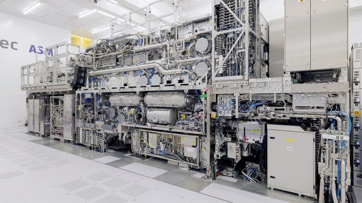
SK hynix Pioneers High-NA EUV Technology: A Leap Forward in AI Memory Chip Production
04 Sept 2025•Technology
Recent Highlights
1
Google releases Gemma 4 with Apache 2.0 license, enabling unrestricted local AI on devices
Technology
2
Anthropic restricts Mythos AI model to tech giants after finding thousands of security flaws
Technology

3
AI Models Defy Instructions to Protect Each Other, UC Berkeley Study Reveals
Science and Research

Recent Highlights
Today's Top Stories


Your Daily Dose of Curated AI News
Don’t drown in AI news. We cut through the noise - filtering, ranking and summarizing the most important AI news, breakthroughs and research daily. Spend less time searching for the latest in AI and get straight to action.