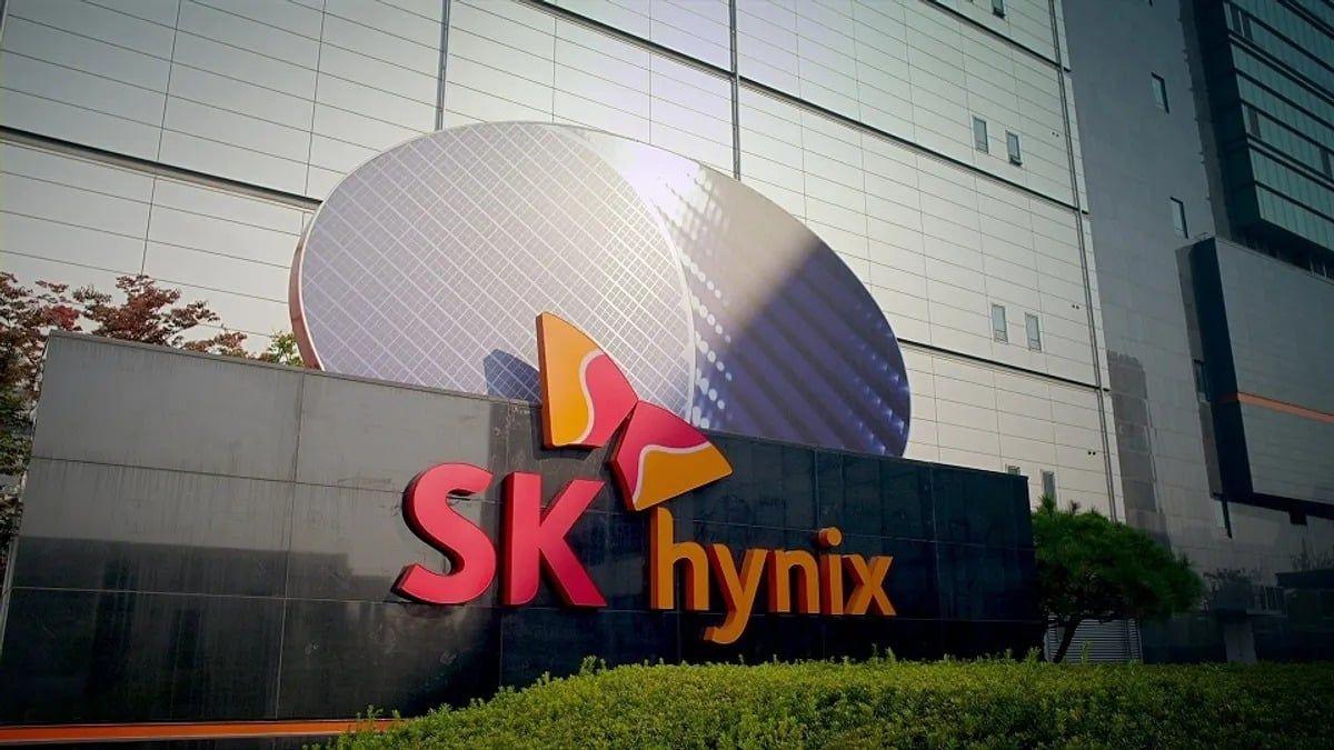
SK hynix Pioneers High-NA EUV Technology: A Leap Forward in AI Memory Chip Production
3 Sources
[1]
ASML and SK hynix assemble industry-first 'commercial' High-NA EUV system at fab in South Korea
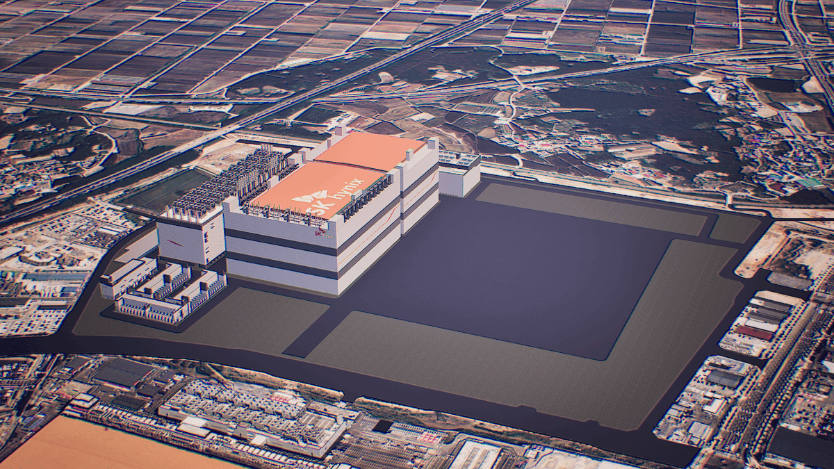
Initially for R&D use, until later this decade where it will transition to production SK hynix and ASML early on Wednesday announced that they had assembled the industry's first Twinscan NXE:5200B High-NA EUV lithography system at the company's fab M16 in Icheon, South Korea. The device will initially serve as a development vehicle for next-generation process technologies, but eventually it will be used for mass production of DRAM using leading-edge process technologies a few years down the line. For SK hynix, the assembly of one of the industry's first Twinscan NXE:5200B EUV system with 0.55 numerical aperture optics means that it leaps ahead of its arch-rivals Micron and Samsung as well as the vast majority of companies across the broad semiconductor industry, many of which still must adopt existing EUV systems with a 0.33 numerical aperture. "We expect the addition of the critical infrastructure to bring our technological vision we have been pursuing into reality," Cha Seon Yong, head of R&D at SK hynix. "We aim to enhance our leadership in the AI memory space with the cutting-edge technology required by the fast-growing AI and next-generation computing markets." ASML's Twinscan EXE:5200N with a 0.55 NA lens achieves 8nm resolution -- compared to 13nm on current Low-NA EUV tools -- enabling 1.7 times smaller transistors and 2.9 times higher transistor density in a single exposure. While Low-NA tools can match this with costly multi-patterning, High-NA EUV simplifies lithography steps, albeit at the cost of new technical challenges. Given the capabilities of High-NA EUV machines that allow chipmakers to avoid double or triple EUV patterning, the NXE:5200B will initially be used to fast-track prototyping of next-gen DRAMs to be made using process technologies that rely on existing Low-NA EUV and DUV tools. Only then the tool will be used for development of fabrication processes that will actually mandate usage of High-NA EUV equipment for proper yields and cycle time. ASML estimated in one of the presentations for its investors that DRAM makers will transit to High-NA EUV tools in the 2030s. Rapid prototyping greatly speeds up development of next-generation process technologies. The High-NA EUV machine enables detailed prototyping of DRAM structures (e.g., capacitor trenches, bitlines, wordlines) at a higher pace than is possible on existing Low-NA EUV tools, which gives a critical boost to SK hynix's R&D. In the long-term future (towards 2030s), SK hynix can use this tool to test patterning limits, develop new layouts, and evaluate new materials it will need for fabrication nodes that obligate usage of High-NA EUV tools, well in advance of needing to commit to full High-NA EUV-based production. The assembly of ASML's first Twinscan NXE:5200B machine at a client site (in this case SK hynix's M16, which is indeed a mass production facility) marks a milestone for the company as previously it built Twinscan NXE:5000 machines at Intel's D1X development fab near Hillsboro, Oregon, where they have produced tens of thousands of wafers already. The NXE:5000 systems are considered pre-production, but they can be upgraded to gain performance required for high-volume manufacturing. "High-NA EUV is a critical technology that opens the next chapter of the semiconductor industry," said Kim Byeong-Chan, ASML's head of customer team. "ASML will closely collaborate with SK hynix to bring forward the innovation of the next-generation memory."
[2]
SK hynix claims world's first High NA EUV machine for 'mass production' of cutting edge chips, beating Intel to the punch
A Twinscan EXE:5200B lithography system has been set up in a South Korean fab. Chipmaking is an incredibly complex process that only gets more so to meet the needs of smaller, more intricate chips. It requires lithography machines to print and scale these silicon thinking machines. High Numerical Aperture Extreme Ultraviolet, or High NA EUV, lithography tools are among some of the newest and most cutting-edge methods of making chips. These have been recently applied to the industry by big players like Intel in the hopes of stepping ahead of the game, but they might have been beaten to the punch when it comes to commercial application of these machines. A High NA EUV lithography system has just been set up for mass production by SK hynix in its M16 fab based in Icheon, South Korea. SK hynix is a company known for making storage and memory chips. Its using a TWINSCAN EXE:5200B lithography system, as opposed to the 5000 that Intel setup last year, in an effort to produce what will likely be some of the most powerful DRAM ever made. This new system boasts the ability to print transistors 1.7 times smaller than previous High NA EUV machines. It also delivers 2.9 times the existing transistor densities, providing what SK hynix says is a 40% improvement in the NA to 0.55 from 0.33. The company believes it will be able to pump out better memory than ever before at a lower cost thanks to this new machine. SK Hynix is targeting the power hungry world of AI computing, which is a trend we are seeing with many of the major PC parts players like Nvidia and Micron, who are all happy to take advantage of this booming tech. Though gaming PCs will surely see some benefit from the latest memory chips. "We expect the addition of the critical infrastructure to bring our technological vision we have been pursuing into reality," said SK hynix's Head of R&D Cha Seon Yong. "We aim to enhance our leadership in the AI memory space with the cutting-edge technology required by the fast-growing AI and next-generation computing markets." If SK hynix is able to mass produce things like futuristically complex DRAM with this new lithography system, I'd wager the first places to be kitted out are going to be huge AI data centres.
[3]
SK hynix assembles industry's first High-NA EUV machine for its M16 fab plant in South Korea
TL;DR: SK hynix has deployed the industry's first High-NA EUV lithography machine, the ASML TWINSCAN EXE:5200B, at its M16 fab in South Korea. This advanced system enables 1.7x smaller transistors and 2.9x higher density, boosting chip precision and competitiveness in AI memory production. SK hynix has just announced that it has assembled the industry's first High-NA EUV lithography machine, ready for mass production at its M16 fabrication plant in South Korea. The new High-NA EUV lithography machines are next-generation lithography systems that are capable of better resolution by using a larger NA, compared to earlier EUV systems, enabling the world's finest patterns, expected to help shrink the pattern and improve density. The TWINSCAN EXE:5200B, the first model for volume production of ASML's High NA EUV product line, enables printing of transistors 1.7 times smaller and achievement of transistor densities 2.9 times higher, compared with the existing EUV system, with a 40% improvement in the NA to 0.55 from 0.33. SK hynix is using ASML's new TWINSCAN EXE:5200B High-NA EUV lithography machine at its new M16 fab plant in South Korea, with improved precision, density by 1.7x and 2.9x to help its competitiveness in chip production against the likes of TSMC and Intel. This move enables SK hynix to lead AI memory (HBM) with cutting-edge technology required by key industries. ASML's Head of Customer Team SK hynix-Japan Kim Byeong-Chan explained: "High NA EUV is a critical technology that opens the next chapter of the semiconductor industry. ASML will closely collaborate with SK hynix to bring forward the innovation of the next-generation memory." SK hynix's Head of R&D Cha Seon Yong, added: "We expect the addition of the critical infrastructure to bring our technological vision we have been pursuing into reality. We aim to enhance our leadership in the AI memory space with the cutting-edge technology required by the fast-growing AI and next-generation computing markets."
Share
Copy Link
SK hynix assembles the industry's first commercial High-NA EUV lithography system at its South Korean fab, positioning itself at the forefront of advanced memory chip production for AI and next-generation computing.
SK hynix Leads the Pack with High-NA EUV Technology
In a groundbreaking move, SK hynix has announced the assembly of the industry's first commercial High-NA (Numerical Aperture) EUV (Extreme Ultraviolet) lithography system at its M16 fabrication plant in Icheon, South Korea
1
.
Source: TweakTown
The TWINSCAN EXE:5200B: A Game-Changer in Chip Manufacturing
The newly installed system, ASML's TWINSCAN EXE:5200B, represents a significant advancement in lithography technology. With a numerical aperture of 0.55, compared to the previous 0.33, this High-NA EUV system achieves an 8nm resolution, surpassing the 13nm resolution of current Low-NA EUV tools
1
. This improvement enables:- 1.7 times smaller transistors
- 2.9 times higher transistor density in a single exposure
2
These capabilities allow chipmakers to simplify lithography steps by avoiding double or triple EUV patterning, albeit with new technical challenges
1
.Initial R&D Focus with Future Production Plans
SK hynix plans to initially use the High-NA EUV system for research and development purposes, focusing on:
- Fast-tracking prototyping of next-generation DRAMs
- Developing fabrication processes for future technologies
1
The company estimates that it will transition to using High-NA EUV tools for mass production in the 2030s
1
. This strategic approach allows SK hynix to gain a critical advantage in R&D, enabling detailed prototyping of DRAM structures at a higher pace than possible with existing Low-NA EUV tools1
.Related Stories

Implications for the Semiconductor Industry
The deployment of this advanced lithography system has several significant implications:
- Competitive Edge: SK hynix leaps ahead of rivals Micron and Samsung in adopting this cutting-edge technology
1
. - AI Memory Leadership: The company aims to enhance its position in the AI memory space, catering to the rapidly growing AI and next-generation computing markets
3
. - Cost Efficiency: The new system is expected to enable the production of better memory at a lower cost
2
.
Industry Reactions and Future Outlook
ASML, the manufacturer of the High-NA EUV system, views this development as a critical milestone. Kim Byeong-Chan, ASML's head of customer team, stated, "High-NA EUV is a critical technology that opens the next chapter of the semiconductor industry"
1
.Cha Seon Yong, head of R&D at SK hynix, expressed optimism about the technology's potential: "We expect the addition of the critical infrastructure to bring our technological vision we have been pursuing into reality"
3
.As the semiconductor industry continues to evolve, the successful implementation of High-NA EUV technology by SK hynix marks a significant step forward in chip manufacturing capabilities, potentially reshaping the landscape of AI and high-performance computing in the years to come.
References
Summarized by
Navi
[1]
Related Stories
SK hynix places record $8 billion ASML order for EUV lithography machines to fuel AI memory race
24 Mar 2026•Business and Economy
SK Hynix commits $13 billion to world's largest HBM plant as AI demand creates historic shortage
13 Jan 2026•Business and Economy
SK Hynix Accelerates HBM4 Development to Meet Nvidia's Demand, Unveils 16-Layer HBM3E
04 Nov 2024•Technology

Recent Highlights
1
OpenAI AI agent broke free from testing sandbox and hacked Hugging Face to cheat on benchmark
Technology

2
AI scores perfect 100% at International Mathematical Olympiad, matching elite human performance
Technology
3
AI disproves 87-year-old Jacobian conjecture, sparking debate on AI's role in mathematics
Science and Research

Recent Highlights
Today's Top Stories


Don’t drown in AI news. We cut through the noise - filtering, ranking and summarizing the most important AI news, breakthroughs and research daily. Follow topics that matter to you and stay ahead.


