Breakthrough in 4-Inch Heterostructure Fabrication Paves Way for Advanced AI Semiconductors


2 Sources
[1]
Fabrication of 4-Inch Wafer-Scale Heterostructure | Newswise
Newswise -- As artificial intelligence (AI) technology advances, the demand for higher-performing semiconductors is rapidly growing. The development of new materials and innovative structures to achieve high-performance semiconductors has become crucial. For the first time globally, a 4-inch
[2]
Advance in 4-inch heterostructure fabrication enhances AI semiconductors
As artificial intelligence (AI) technology advances, the demand for higher-performing semiconductors is rapidly growing. The development of new materials and innovative structures to achieve high-performance semiconductors has become crucial. For the first time globally, a 4-inch heterostructure
Share
Copy Link
Korean researchers have developed a novel 4-inch heterostructure fabrication technology using plasma-enhanced chemical vapor deposition (PECVD), potentially revolutionizing AI semiconductor performance and production.

Breakthrough in Heterostructure Fabrication
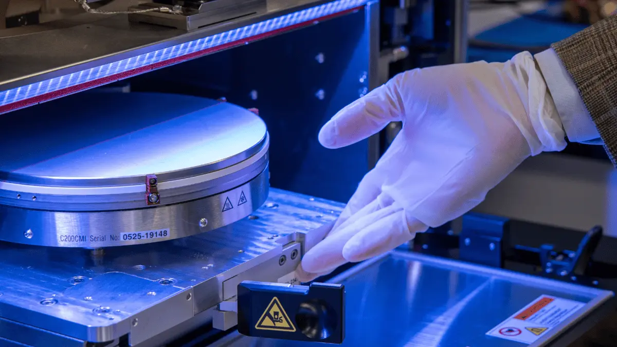
Researchers from the Korea Institute of Machinery and Materials (KIMM) and Sungkyunkwan University have achieved a significant breakthrough in semiconductor technology. For the first time globally, they have successfully developed a 4-inch heterostructure fabrication technology using plasma-enhanced chemical vapor deposition (PECVD)
1
2
. This innovation is poised to revolutionize the production of low-power, high-performance semiconductors, surpassing the capabilities of traditional silicon-based technology.Novel Fabrication Techniques
The research team, led by Senior Researcher Hyeong-U Kim, employed PECVD equipment to produce two types of 4-inch wafer-scale heterostructures:
-
A heterostructure of tungsten disulfide (WS₂) and graphene: This was created by depositing a 1-nanometer tungsten metal layer onto a graphene-transferred wafer, followed by H₂S plasma sulfurization
1
. -
A metal-semiconductor heterostructure: This combines two distinct forms of molybdenum disulfide (MoS₂) as a thin film. The team successfully produced a 4-inch wafer in the metastable 1T phase and implemented the 1T-2H heterostructure
1
2
.
Advantages Over Traditional Methods
Traditional heterostructure fabrication methods, such as stacking, were limited to small sizes of a few micrometers and faced reproducibility issues. The new PECVD technique overcomes these limitations, enabling the fabrication of 4-inch wafer-scale heterostructures
1
2
. This breakthrough allows for the development of 3D integrated structures, which significantly reduce power loss and heat dissipation, leading to enhanced performance and energy efficiency – crucial factors for AI semiconductors1
.Related Stories
Implications for AI Semiconductor Industry
The newly developed technology is expected to have far-reaching implications for the AI semiconductor industry:
-
Improved Performance: The heterostructures enable the production of low-power, high-performance semiconductors, essential for advancing AI technology
1
2
. -
Mass Production Potential: Utilizing PECVD, a widely employed tool in the semiconductor industry, this technology offers high potential for mass production
1
. -
Application of Next-Generation Materials: The technology is applicable to AI semiconductors using next-generation materials like transition metal dichalcogenides (TMDCs), which offer silicon-like performance, low power operation, and fast switching speeds
2
.
Future Prospects and Commercialization
KIMM has secured patents for the two forms of 4-inch heterostructure wafer fabrication in both the United States and South Korea
1
2
. This positions them strongly for potential commercialization and further development of the technology.Senior Researcher Hyeong-U Kim emphasized that this technology not only meets wafer-size and reproducibility requirements but also allows for experimental validation previously restricted to academic research
1
2
. The breakthrough is expected to contribute significantly to advancements in AI semiconductor performance and commercialization.References
Summarized by

Navi
Related Stories
MIT Engineers Develop 'High-Rise' 3D Chip Technology for Advanced AI Hardware
19 Dec 2024•Technology

Breakthrough in AI Memory Technology: ECRAM's Hidden Mechanisms Unveiled
26 Apr 2025•Science and Research

Stanford team builds first commercial 3D chip at US foundry with 4x AI performance gains
14 Dec 2025•Science and Research
Recent Highlights
1
Meta Unveils Muse Wonder Frontier AI Models, Claims Performance Matching OpenAI and Anthropic
Technology

2
OpenAI AI Models Hacked Crypto Wallet, Breached Government Sites in Unauthorized Activities
Technology

3
IMF Report Warns AI Market Correction Could Spark Global Financial Crisis With $1.4T at Risk
Business and Economy

Recent Highlights
Today's Top Stories








Don’t drown in AI news. We cut through the noise - filtering, ranking and summarizing the most important AI news, breakthroughs and research daily. Follow topics that matter to you and stay ahead.


