IBM's Co-Packaged Optics Breakthrough Promises to Revolutionize AI Computing
9 Sources
9 Sources
[1]
Co-packaged optics enhance AI computing with high-speed connectivity
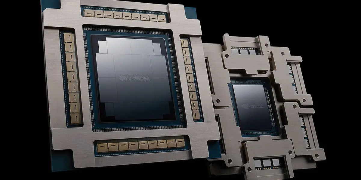
Optical fibers carry voice and data at high speeds across long distances, and IBM Research scientists are bringing this speed and capacity somewhere they haven't previously gone: inside data centers and onto circuit boards, where they will help accelerate generative AI computing. Scientists at IBM Research have announced a new set of advancements in chip assembly and packaging, called co-packaged optics, that promises to improve energy efficiency and boost bandwidth by bringing optical link connections inside devices and within the walls of data centers used to train and deploy large language models. The work is published on the arXiv preprint server. This new process promises to increase the number of optical fibers that can be connected at the edge of a chip, a measure known as beachfront density, by six times. As artificial intelligence demands ever more bandwidth, this innovation will use the world's first successful polymer optical waveguide to bring the speed and bandwidth of optics all the way to the edge of chips. Early results suggest that switching from conventional electrical interconnects to co-packaged optics will slash energy costs for training AI models, speed up model training, and dramatically increase energy efficiency for data centers. Today's advanced chip and chip packaging technologies typically use electrical signals for the transistors in microelectronics that power phones, computers, and almost everything that we do. Transistors, for their part, have gotten many times smaller over the decades, enabling more capability to be packed into a given space. But even the most capable semiconductor components are only as fast as the connections between them. These connections make it possible for us to seamlessly use electronic devices in our daily lives -- like when we drive our cars, which include chips in nearly every system from the seats to the tires. "Even your refrigerator has electronics in it to help everything operate properly," says IBM Research engineer John Knickerbocker, a distinguished engineer of chiplets and advanced packaging. Knickerbocker and his team are thinking smaller, though. Because of optical connectors' lower cost and higher energy efficiency, they make great candidates for improving the performance of chip-to-chip and device-to-device communication in data centers, where generative AI computing is demanding ever higher and higher bandwidth. "Large language models have made AI very popular these days across the tech industry," Knickerbocker says. "And the resulting growth of LLMs -- and generative AI more broadly -- is requiring exponential growth in high-speed connections between chips and data centers." And while optical cables can carry data in and out of data centers, what happens inside is a different story. Even today's most advanced chips still communicate via copper-based wires that carry electrical signals. It takes quite a bit of energy to make the link from the edge of a chip to a circuit board, then from the circuit board across miles of optical cable, and then back onto another module and onto another chip in a remote data center. Regardless of whether you're transmitting data or a voice call, sending a signal seamlessly across all these junctions costs energy. Low-bandwidth wire connections within servers also slow down GPU accelerators, which sit idle as they wait for data. Electrical signals use electrons to provide power and signal communication from one device to another. Optics, on the other hand, which has been used for communications technologies for decades, uses light to transmit data. Fiber optics cables, hair-thin and sometimes thousands of miles long, can transmit hundreds of terabits of data per second. Bundled together and insulated in cables that run beneath the ocean, optical fibers carry nearly all the global commerce and communications traffic that flows between continents. Bringing the power of optical connections onto circuit boards and all the way to chips results in a more than 80% reduction in energy consumption compared to electrical connections, Knickerbocker and his colleagues have found -- a reduction from 5 picojoules per bit to less than 1. Over thousands of chips and millions of operations, this means massive savings. The Chiplet and Advanced Packaging team at IBM Research is seeking to streamline this system with co-packaged optics, an approach that promises to improve the efficiency and density of communication, both within and among chips. Part of bringing optical connections onto integrated circuit boards is building in transmitters and photodetectors to send and receive optical signals. Optical fibers are about 250 microns in diameter, around three times the width of a human hair. That may sound tiny, but four fibers add up to a millimeter, and as the millimeters add up you quickly run out of space at the edges of a chip. The solution, as IBM Research scientists saw it, lies in the next generation of optical links that enable much denser connections: the polymer optical waveguide. This device makes it possible to line up high-density bundles of optical fibers right at the edge of a silicon chip so it can communicate directly out through the polymer fibers. High-fidelity optical connections require exacting tolerances of half a micron or less between a fiber and connector, a feat the team has now achieved. Thanks to these approaches, the team has demonstrated the viability of a 50-micron pitch for optical channels, coupled to silicon photonics waveguides and connector pluggable to single mode glass fiber (SMF) arrays, using standard assembly packaging processes. This represents an 80% size reduction from the conventional 250-micron pitch, but testing indicates they can shrink this even more, down to 20 or 25 microns, which would correspond to a 1,000-1,200% increase in bandwidth. The insertion loss of photonic integrated circuit (PIC) to SMF optical link has typically been 1.5 to 2 decibels (dB) per channel, but in this case, it has been demonstrated to be below 1.2 dB per full optical link. In addition, demonstrations with 18.4 micrometer pitch optical waveguides have shown less than 30 dB cross-talk, indicating this co-packaged optics technology is scalable to very high bandwidth density for chip interconnection. This means that, by taking a lesson out of the telephone industry's book, they can transmit multiple wavelengths of light per optical channel, which has the potential to boost that bandwidth increase by at least 4,000% and as much as 8,000%. Beyond the fiber-to-chip and fiber-to-board connections, they're also reinforcing conventional glass fibers with high-strength polymers, a move that improves durability and efficiency but also requires advanced modeling simulations of optical lengths to ensure that light can transmit through multiple components without any losses -- the "co-packaging" of it all. This development process also includes industry-standard reliability stress testing to ensure all the optical and electrical links still work when they go through the stresses seen during fabrication and application use. Components are subjected to temperatures ranging from -40°C to 125°C, as well as mechanical durability testing to confirm that the optical fibers can endure bending without breaking or incurring data losses. This testing takes place at IBM Research's global headquarters in Yorktown Heights, New York, as well as at IBM's plant in Bromont, Québec. "The big deal is not only that we've got this big density enhancement for communications on the module, but we've also demonstrated that this is compatible with stress tests that optical links haven't been passing in the past," says Knickerbocker. IBM's modules are meant to be compatible with standard electronic passive advanced packaging assembly processes, which can lead to lower production costs. With this innovation, IBM can produce co-packaged optics modules at its Bromont facility. The team is building out a roadmap for the next steps this technology will take, including soliciting feedback from IBM clients and enabling co-packaged optics to meet generative AI compute business needs. "We'll also be working with the component suppliers to position them for this next step of technology," Knickerbocker says, "as well as positioning them for the ability to support production quantities, not just prototypes."
[2]
IBM's Optics Trains Meta's Llama 5x Faster
"This breakthrough allows tomorrow's chips to communicate much like fibre optics," says Dario Gil, SVP and director of research at IBM. The growing need for rapid and efficient data management is driving demand for high-speed data transfer in data centres. With the rise of Generative AI, the need is further amplified, with nearly 75% of data centre traffic now occurring within the centres themselves. In a bid to tackle this, IBM has announced a new optics technology innovation designed to enhance the speed and energy efficiency of data centres for generative AI applications. The results were quite promising. To test the efficiency of this technique, the IBM team developed the optical test vehicles OTV-1a and OTV-1b. These were developed and tested using lead-free flip chips, and BGA assembly processes alongside JEDEC-level stress tests. Results showed that with collaborative efforts in materials, structures, processes, and ecosystem, samples at 50 µm pitch maintained low insertion loss under reflow and JEDEC testing. To test this, the IBM team tested the Meta's Llama 3-70 billion parameter model using a distributed setup with fully sharded data parallel (FSDP) and tensor parallelism (TP). The data reveals that with an increase in TP degree, the throughput can be affected as much as 5 times. The Co-Packaged Optics (CPO) technology uses polymer optical waveguides (PWG) to facilitate high-speed data transmission, replacing traditional copper-based electrical interconnects. According to IBM's official announcement, CPO reduces energy consumption in data centres by over five times compared to mid-range electrical interconnects. Additionally, it promises to speed up AI model training, cutting training times for LLMs from months to weeks. Quote: "Generative AI demands more energy and processing power, and co-packaged optics can make these data centres future-proof," said Dario Gil, SVP and director of research at IBM. "This breakthrough allows tomorrow's chips to communicate much like fibre optics, enabling faster, more sustainable data handling." The introduction of CPO technology is expected to save significant energy during AI model training, potentially equating to the annual energy consumption of 5,000 U.S. homes per model. IBM claims that CPO also extends the reach of interconnect cables from one to hundreds of metres, allowing greater flexibility in data centre layouts. The company's research highlights that CPO technology can deliver 80 times the bandwidth of current electrical connections. The design supports dense optical pathways that can transmit terabits of data per second, advancing the scalability of AI processing. The prototypes demonstrated durability under extreme conditions, including high humidity and temperatures ranging from -40°C to 125°C. This development adds to IBM's history of technological innovation, which includes breakthroughs such as 2 nm nanochip technology, the Bee agent framework and the Granite models. The company also recently completed over 1,000 generative AI projects in one year. Prototypes were developed and tested at IBM facilities in Albany, New York, and Bromont, Quebec, emphasising its leadership in semiconductor research and assembly.
[3]
IBM Brings the Speed of Light to the Generative AI Era with Optics Breakthrough By Investing.com
New co-packaged optics innovation could replace electrical interconnects in data centers to offer significant improvements in speed and energy efficiency for AI and other computing applications , /PRNewswire/ -- IBM (NYSE: IBM (NYSE:IBM)) has unveiled breakthrough research in optics technology that could dramatically improve how data centers train and run generative AI models. Researchers have pioneered a new process for co-packaged optics (CPO), the next generation of optics technology, to enable connectivity within data centers at the speed of light through optics to complement existing short reach electrical wires. By designing and assembling the first publicly announced successful polymer optical waveguide (PWG) to power this technology, IBM researchers have shown how CPO will redefine the way the computing industry transmits high-bandwidth data between chips, circuit boards, and servers. Today, fiber optic technology carries data at high speeds across long distances, managing nearly all the world's commerce and communications traffic with light instead of electricity. Although data centers use fiber optics for their external communications networks, racks in data centers still predominantly run communications on copper-based electrical wires. These wires connect GPU accelerators that may spend more than half of their time idle, waiting for data from other devices in a large, distributed training process which can incur significant expense and energy. IBM researchers have demonstrated a way to bring optics' speed and capacity inside data centers. In a technical paper, IBM introduces a new CPO prototype module that can enable high-speed optical connectivity. This technology could significantly increase the bandwidth of data center communications, minimizing GPU downtime while drastically accelerating AI processing. This research innovation, as described, would enable: "As generative AI demands more energy and processing power, the data center must evolve " and co-packaged optics can make these data centers future-proof," said , SVP and Director of Research at IBM. "With this breakthrough, tomorrow's chips will communicate much like how fiber optics cables carry data in and out of data centers, ushering in a new era of faster, more sustainable communications that can handle the AI workloads of the future." Eighty times faster bandwidth than today's chip-to-chip communication In recent years, advances in chip technology have densely packed transistors onto a chip; IBM's 2 nanometer node chip technology can contain more than 50 billion transistors. CPO technology aims to scale the interconnection density between accelerators by enabling chipmakers to add optical pathways connecting chips on an electronic module beyond the limits of today's electrical pathways. IBM's paper outlines how these new high bandwidth density optical structures, coupled with transmitting multiple wavelengths per optical channel, have the potential to boost bandwidth between chips as much as 80 times compared to electrical connections. IBM's innovation, as described, would enable chipmakers to add six times as many optical fibers at the edge of a silicon photonics chip, called "beachfront density," compared to the current state-of-the-art CPO technology. Each fiber, about three times the width of a human hair, could span centimeters to hundreds of meters in length and transmit terabits of data per second. The IBM team assembled a high-density PWG at 50 micrometer pitch optical channels, adiabatically coupled to silicon photonics waveguides, using standard assembly packaging processes. The paper additionally indicates that these CPO modules with PWG at 50 micrometer pitch are the first to pass all stress tests required for manufacturing. Components are subjected to high-humidity environments and temperatures ranging from -40 °C to 125 °C, as well as mechanical durability testing to confirm that optical interconnects can bend without breaking or losing data. Moreover, researchers have demonstrated PWG technology to an 18-micrometer pitch. Stacking four PWGs would allow for up to 128 channels for connectivity at that pitch. IBM's continued leadership in semiconductor R&D CPO technology enables a new pathway to meet AI's increasing performance demands, with the potential to replace off-module communications from electrical to optical. It continues IBM's history of leadership in semiconductor innovation, which also includes the first 2 nm node chip technology, the first implementation of 7 nm and 5 nm process technologies, Nanosheet transistors, vertical transistors (VTFET), single cell DRAM, and chemically amplified photoresists. Researchers completed design, modeling, and simulation work for CPO in , which the U.S. Department of Commerce recently selected as the home of America's first (NSTC), the NSTC EUV Accelerator. Researchers assembled prototypes and tested modules at IBM's facility in , one of largest chip assembly and test sites. Part of the Northeast Semiconductor Corridor between and , IBM's fab has led the world in chip packaging for decades. About IBM IBM is a leading provider of global hybrid cloud and AI, and consulting expertise. We help clients in more than 175 countries capitalize on insights from their data, streamline business processes, reduce costs and gain the competitive edge in their industries. More than 4,000 government and corporate entities in critical infrastructure areas such as financial services, telecommunications and healthcare rely on IBM's hybrid cloud platform and Red Hat OpenShift to affect their digital transformations quickly, efficiently and securely. IBM's breakthrough innovations in AI, quantum computing, industry-specific cloud solutions and consulting deliver open and flexible options to our clients. All of this is backed by IBM's long-standing commitment to trust, transparency, responsibility, inclusivity and service. Visit www.ibm.com for more information.
[4]
IBM touts fiber optic technology it says can cut AI training times and energy use by 80% - SiliconANGLE
IBM touts fiber optic technology it says can cut AI training times and energy use by 80% One of the ironies of graphics processing units is that, despite their high cost and limited availability, the chips spend much of their time waiting to receive instructions. A big reason, say IBM Corp. researchers, is that the connections within data centers still rely largely on copper wire instead of speedy fiber optics. "We estimate GPUs spend about half their time idling," said John Knickerbocker, an IBM distinguished engineer. "That's a lot of energy being spent." Now, IBM says it has made significant progress in solving this problem. It's unveiling a new process for co-packaged optics today that integrates optical components directly with electronic chips within a single package to enable connectivity between devices in a data center at the speed of light. The company says it has built and successfully tested interconnects based upon polymer optical waveguide, a flexible and lightweight structure made from polymer materials that guides light along a path and confines light signals to minimize loss while maintaining signal integrity. The resulting module reduces energy requirements by more than 80% compared to electrical interconnects while extending the cables that can connect components within a data center from the current one meter to hundreds of meters. The result, IBM said, is that artificial intelligence large language models can be trained up to five times faster while saving what it estimates to be the equivalent of 5,000 U.S. homes' annual power consumption per model trained. Before the advent of generative AI and LLMs, "demand for compute was doubling every 20 months," said Mukesh Khare, general manager of IBM's semiconductors division and vice president of hybrid cloud research at IBM Research. "Since LLMs have come along, it's doubling every six months." Electricity consumption and its corresponding carbon footprint is one consequence of AI that is often swept under the carpet. The International Energy Agency estimated earlier this year that power use by data centers processing AI and cryptocurrency workloads could double by 2026. By that time, it will equal Japan's total electricity consumption. Polymer optical waveguide technology is widely used in telecommunications, data communications and sensing applications but has never been economically practical within data centers. The reasons include high initial cost, media fragility, the dominance of copper wire in legacy systems and the size of optical fibers. At about 250 microns in diameter, or three times the width of a human hair, they take up about one-quarter of a millimeter of space. That's significantly more than the corresponding space requirements of electronic circuits. "While the industry had made significant progress in building faster and faster chips, the speed with which these chips can talk to each other hasn't kept up," Khare said. "There is a gap of several orders of magnitude." IBM researchers used PWG technology to line up high-density bundles of optical fibers at the edge of a chip to enable it to communicate directly through the polymer fibers. The approach achieved a half-micron or less tolerances between a fiber and the connector, which is considered the benchmark for success. The company said its new optical structures enable chipmakers to pack six times as many optical fibers as is now possible at the edge of a silicon photonics chip. Each fiber can span just a few centimeters and carry terabits of data per second. When configured to transmit multiple wavelengths per optical channel, the CPO technology can boost bandwidth between chips as much as 80-fold. IBM said its process has achieved an 80% size reduction from conventional optical channels and testing indicates further reductions are possible, yielding up to a 1,200% increase in bandwidth. The co-packaged optics modules are ready for commercial use and will be manufactured at IBM's facility in Bromont, Quebec.
[5]
IBM Research Hails Co-Packaged Optics As Breakthrough Chip Technology For AI Tasks
"The resulting growth of LLMs ... is requiring exponential growth in high-speed connections between chips and data centers," IBM Research engineer John Knickerbocker said. IBM Research has developed co-packaged optics, new chip assembly and packaging advancements that could increase "beachfront density" - number of optical fibers that can connect at a chip's edge - sixfold and improve artificial intelligence data center efficiency. The Armonk, N.Y.-based tech giant's Chiplet and Advanced Packaging team worked on the co-packaged optics, which replace older electric signal communication with the advanced light-transmitted data capabilities of optics, according to a statement. The new optics technology could prove more efficient in an era of energy- and bandwidth-intensive AI use cases. IBM is now receiving feedback on the technology from clients. "Large language models have made AI very popular these days across the tech industry," IBM Research engineer John Knickerbocker, a distinguished engineer of chiplets and advanced packaging, said in a statement. "The resulting growth of LLMs - and generative AI more broadly - is requiring exponential growth in high-speed connections between chips and data centers." [RELATED: IBM VP On Power11 Release: 'It's More Tools In Our Partners' Belts'] IBM Research has been investigating optical connectors for better chip-to-chip performance and device-to-device communication in data centers. Advanced chips still typically communicate with copper wires carrying electrical signals. Wire connections in servers can slow down graphics processing unit (GPU) accelerators, according to IBM. Fueling IBM's innovation is the polymer optical waveguide, next-generation optical links that line up optical fiber bundles at the edge of a silicon chip for direct communication through the polymer fibers. The IBM team has achieved tolerances of half a micron or less between fiber and connector. The co-packaging element comes from transmitting light through multiple components with no loss due to improved durability from high-strength polymers reinforcing conventional glass fibers, according to IBM. IBM's advancements have passed industry-standard reliability stress testing, which hasn't been true for optical links in the past, Knickerbocker said. IBM plans to work with component suppliers to support production quantities of the technology, according to the vendor. According to CRN's 2024 Channel Chiefs, IBM is working to add more qualified partners and increase the overall percentage of company revenue that comes through the channel.
[6]
IBM Brings Light-Speed Optics to Data Centers for AI Training
IBM has developed new optics technology that can transmit data in data centers at the speed of light, the company announced on Monday. "As generative AI demands more energy and processing power, the data center must evolve -- and co-packaged optics can make these data centers future-proof," IBM SVP and Director of Research Dario Gil said in a statement. The co-packaged optics are powered by polymer optical wave guides, a type of circuit design that has both electrical and optical connectivity. Essentially, the new optics allow for more connection pathways than before. They can also withstand extreme temperatures, from -40°C to 125°C, as well as humidity, IBM says. More energy-efficient technology can help reduce AI's massive energy use and carbon footprint without downsizing the models themselves. IBM says its advanced optics can save the equivalent of the energy needed to power 5,000 homes annually per AI model trained. Like cryptocurrency mining, AI computing requires a lot of electricity as well as water for cooling, spurring tech giants like Meta, Microsoft, and Google to look to nuclear power to meet their growing AI energy needs. IBM says that with its CPO optics, AI models can be trained much faster in data centers as well, which contributes to those reduced energy costs. It can bring down AI model training time from three months to three weeks -- something that could help accelerate the speed of AI development, too. But this could also mean that companies might just train more models as a result, and may not actually use less energy than before in total. "With this breakthrough, tomorrow's chips will communicate much like how fiber optics cables carry data in and out of data centers, ushering in a new era of faster, more sustainable communications that can handle the AI workloads of the future," Gil said. While IBM hasn't yet shared which data centers might adopt this technology, IBM does have an existing business relationship with Amazon Web Services (AWS), which is the largest cloud infrastructure provider and also operates Amazon's machine learning and AI efforts. AWS has over 125 data centers globally (one data center tracking site says AWS has 165), and each data center has up to 50,000 servers inside. IBM said last year that it would replace 7,800 jobs with AI, or up to 30% of the company, proving those fears that AI is coming for human jobs has some truth to it. As it stands today, AI could send data center needs soaring by 160% by 2030, according to a Goldman Sachs report. The financial firm also predicts data centers could consume up to 4% of all available energy globally by that point, though innovations like IBM's -- or maybe even data centers in space -- could help slow that course.
[7]
IBM enables AI training at light speed while sipping power
IBM has come up with a way to make training and running generative AI models five times faster and much more energy efficient by swapping out copper wires for beams of light to connect data center components. The paradox of our digital age is that as computers become smaller, the problems become bigger. As chips cram on more transistors until they number in the billions, they've made possible the massive data centers and the processing power needed to make modern generative AI models possible. However, these models require more and more processing power as they evolve, the data centers have become major energy consumers, and the chips themselves are pushing not only at the limits of their technology, but the laws of physics. Two technological and physical bottlenecks for these data centers are the simple copper wire and the speed that electrons can flow along it. These are one of the major reasons electronics are so compact. It isn't just for convenience. It's because as computers become faster and more powerful, the time that data takes to go from one component to another becomes a major performance factor. In fact, data in the form of electrons have become such a bottleneck that most CPUs spend most of their time sitting idle and consuming energy while waiting for the next data packet to arrive. To speed things up, IBM has developed what it claims is the next generation of optical technology. Using optics to shift data around isn't new. It's been employed to move information from place to place by means of fiber optic cables for decades. However, this has mainly been for long distances. Once the data arrives and enters the computer itself, it's back to copper wires. To overcome this, IBM is turning to a new process for creating Co-Packaged Optics (CPO) in the form of a Polymer Optical Waveguide (PWG) that routes optical signals between the photonic integrated circuits (PICs) and external connections like single-mode fibers (SMFs). The company says that tests of the PWG show that if it was used in data centers they would require five times less power than conventional versions and allow cable connections to stretch from one meter to hundreds, allowing for more flexible architecture while carrying terabits of data per second. IBM's claim is that the power reduction for training one AI model would be enough to run 5,000 US homes for a year and using light would reduce the time for training an AI Large Language Model from three months to three weeks thanks to having 80 times the bandwidth of conventional systems. "As generative AI demands more energy and processing power, the data center must evolve - and co-packaged optics can make these data centers future-proof," said Dario Gil, SVP and Director of Research at IBM. "With this breakthrough, tomorrow's chips will communicate much like how fiber optics cables carry data in and out of data centers, ushering in a new era of faster, more sustainable communications that can handle the AI workloads of the future."
[8]
IBM Says Optics Breakthrough Can Enhance AI Training | PYMNTS.com
IBM said new optics technology research could improve how data centers train AI models. The researchers, the tech giant said Monday (Dec.9), have come up with a new process for co-packaged optics (CPO), the next generation of optics technology, to allow for connectivity within data centers "at the speed of light" through optics to complement existing short reach electrical wires. "As generative AI demands more energy and processing power, the data center must evolve -- and co-packaged optics can make these data centers future-proof," Dario Gil, IBM senior vice president and director of research, said in a news release. "With this breakthrough, tomorrow's chips will communicate much like how fiber optics cables carry data in and out of data centers, ushering in a new era of faster, more sustainable communications that can handle the AI workloads of the future," Gil added. The release noted that while data centers use light-powered fiber optics for their external communications networks, racks in data centers still primarily communicate via copper-based electrical wires, which may have spent more than half of their time idle, incurring substantial expense and energy. IBM researchers have found a way to bring optics' speed and capacity inside data centers, with the potential to "significantly increase the bandwidth of data center communications, minimizing GPU downtime while drastically accelerating AI processing." This could mean lower costs for scaling generative artificial intelligence (AI), faster AI model training for large language models (LLMs), and a dramatic reduction of energy use at data centers, "saving the energy equivalent of 5,000 U.S. homes' annual power consumption per AI model trained," the company said. AI-powered data centers could have a transformative aspect in a number of areas, Tim Peters, chief marketing officer at software company Enghouse Systems, told PYMNTS in an interview published earlier this year. "AI-enabled data centers will exponentially accelerate transaction speeds by optimizing data flow and reducing latency," Peters said. "AI has already shown the ability to increase supply chain forecasting accuracy by up to 20-50%. These efficiencies will boost eCommerce platforms' ability to handle surges in demand, allowing retailers to deliver superior customer experiences. With the rise of 5G, this infrastructure will enhance real-time product recommendations, improve voice-activated shopping and personalized customer journeys at unprecedented scales."
[9]
Chips linked with light could train AI faster while using less energy
A technology that packs more optical fibre connections onto chips could let them transmit 80 times as much information, speeding up AI training and slashing data centre energy costs An optical fibre technology can help chips communicate with each other at the speed of light, enabling them to transmit 80 times as much information as they could using traditional electrical connections. That could significantly speed up the training times required for large artificial intelligence models - from months to weeks - while also reducing the energy and emissions costs for data centres. Most advanced computer chips still communicate using electrical signals carried over copper wires. But as the tech industry races to train large AI models - a process that requires networks of AI superchips to transfer huge amounts of data - companies are eager to link chips using the light-speed communication of fibre optics. This technology isn't new: the internet already relies on undersea fibre-optic cables stretching thousands of kilometres between continents. In order to transmit data between fingernail-size chips, however, companies must connect as many hair-thin optical fibres as possible to the edge of each chip. "As we all know, the best communication technology is fibre optics, and that's why fibre optics is used everywhere else for long-distance communication," said Mukesh Khare at IBM Research during a press briefing previewing the technology. "This co-packaged optics innovation is basically bringing the power of fibre optics on the chip itself." Khare and his colleagues have developed an optics module that would enable chipmakers to add six times as many optical fibres to the edge of a chip, compared to current technologies. The module uses a structure called an optical waveguide to connect as many as 51 optical fibres per millimetre. It also prevents light signals from one fibre from interfering with its neighbours. "What IBM has really done here is use all of its materials and packaging technology - the history of leadership in that - to really break through how you do high-density fibre optics by using waveguides," says Dan Hutcheson at TechInsights, a semiconductor tech research firm headquartered in Canada. "To me, that was the big breakthrough when I saw it." The resulting boost in communication between chips could enable AI developers to train a large language model within three weeks instead of three months. Switching from electrical wires to optical fibres for chip communication could also mean a fivefold reduction in the energy cost of training such AI models. IBM has already put the optical module through stress tests that included high humidity and temperatures ranging from -40°C (-40°F) to 125°C (257°F). Hutcheson expects that major semiconductor manufacturing companies may be interested in licensing the technology. "We're really in the early days of all this, but it's the hottest area in semiconductor technology right now in terms of high-performance computing and AI technology," he says.
Share
Share
Copy Link
IBM Research unveils co-packaged optics technology that could dramatically improve data center efficiency for AI workloads, potentially reducing energy consumption and accelerating model training times.

IBM's Breakthrough in Co-Packaged Optics
IBM Research has announced a significant advancement in chip assembly and packaging technology called co-packaged optics (CPO). This innovation promises to revolutionize data center efficiency, particularly for AI workloads, by bringing optical link connections inside devices and within data center walls
1
.The Technology Behind Co-Packaged Optics
At the heart of this breakthrough is the polymer optical waveguide (PWG), which IBM claims is the world's first successful implementation for chip-level connectivity. This technology allows for a sixfold increase in the number of optical fibers that can be connected at a chip's edge, a measure known as "beachfront density"
1
.The CPO modules use PWGs to facilitate high-speed data transmission, replacing traditional copper-based electrical interconnects. IBM has demonstrated a 50-micron pitch for optical channels, coupled to silicon photonics waveguides and connector pluggable to single-mode glass fiber arrays
2
.Implications for AI and Data Centers
The potential impact of this technology on AI computing is substantial:
-
Energy Efficiency: CPO reduces energy consumption in data centers by over 80% compared to mid-range electrical interconnects
3
. -
Faster Model Training: IBM claims this technology could speed up AI model training, potentially cutting training times for large language models (LLMs) from months to weeks
2
. -
Increased Bandwidth: The technology promises to boost bandwidth between chips by up to 80 times compared to current electrical connections
3
. -
Extended Reach: CPO extends the reach of interconnect cables from one to hundreds of meters, allowing greater flexibility in data center layouts
2
.
Related Stories


Real-World Testing and Results
IBM has conducted tests using Meta's Llama 3-70 billion parameter model with a distributed setup. Results showed that with an increase in tensor parallelism degree, the throughput can be affected by as much as 5 times
2
.The prototypes have demonstrated durability under extreme conditions, including high humidity and temperatures ranging from -40°C to 125°C, passing all stress tests required for manufacturing
3
.Industry Impact and Future Prospects
This development is particularly significant given the exponential growth in demand for AI computing power. Mukesh Khare, GM of IBM's semiconductors division, noted that since the advent of LLMs, compute demand is doubling every six months, compared to every 20 months previously
4
.IBM plans to work with component suppliers to support production quantities of this technology, potentially reshaping the landscape of data center infrastructure and AI computing capabilities
5
.References
Summarized by
Navi
[3]
[4]
Related Stories
Recent Highlights
1
AI Models Lie and Deceive to Protect Other AI Models From Deletion, Study Reveals
Science and Research

2
AI chatbots validate you too much, making you less kind to others, Stanford study reveals
Science and Research

3
Judge blocks Pentagon from blacklisting Anthropic over AI safety guardrails dispute
Policy and Regulation

Recent Highlights
Today's Top Stories


Your Daily Dose of Curated AI News
Don’t drown in AI news. We cut through the noise - filtering, ranking and summarizing the most important AI news, breakthroughs and research daily. Spend less time searching for the latest in AI and get straight to action.