Nvidia Unveils Vera Rubin Superchip: Six-Trillion Transistor AI Platform Set for 2026 Production
7 Sources
7 Sources
[1]
Nvidia Offers First Look at Vera Rubin Superchip
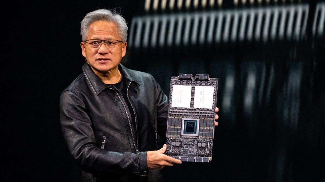
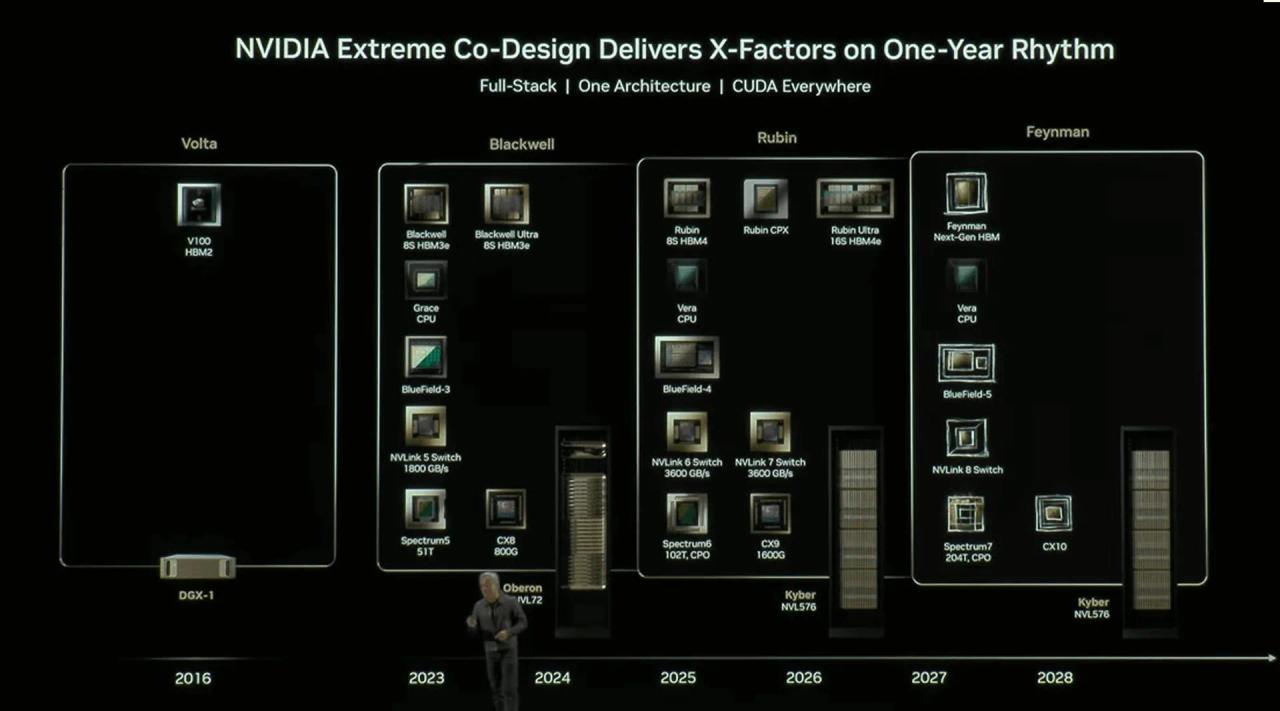
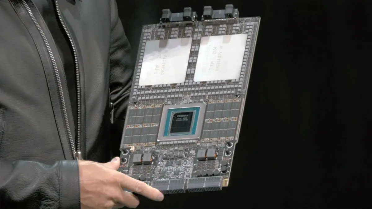
Nvidia CEO Jensen Huang (Credit: Kent Nishimura/Bloomberg via Getty Images) Don't miss out on our latest stories. Add PCMag as a preferred source on Google. While batting away deepfakes, Nvidia's GTC DC show showed off the superchip platform that will power next-generation data centers: Vera Rubin. This single-board system that combines an 88-core Vera CPU with twin Rubin GPUs will be the backbone of Nvidia's 2026 strategy to continue powering the AI revolution, and its next trillion dollars in valuation. "This is the next-generation Rubin," CEO Jensen Huang said at GTC. "While we are shipping GB300, we are preparing Rubin to be in production this time next year, maybe slightly earlier. This is just an incredibly beautiful computer," with 100 Petaflops of FP4 performance for AI. Although Nvidia is facing some skepticism over its performance claims of late, there's no denying that Vera Rubin will be the most powerful "Superchip" ever made when it hits mass production in 2026. It's built using next-generation architectures for Nvidia's CPU and GPU designs, and more than doubles the number of CPU cores over the current-generation GB200 Grace Blackwell flagship. Each Rubin GPU has access to 288GB of HBM4 memory, with the GPUs and CPUs linked together using an enhanced NVLINK-C2C with increased throughput, as per VideoCardz. All of that equates to a huge increase in performance over existing Grace Blackwell systems that Nvidia has been hyping so much in its big AI data center deals this year. The full NVL144 system will be able to offer 3.6 Exaflops FP4 inference and 1.2 Exaflops FP8 in training workloads. That works out to around 3.3 times faster than Nvidia's GB300 NVL72 platform. As if that wasn't enough, Nvidia teased what's coming after what's coming next, in the form of Rubin Ultra NVL576. Slated to debut sometime in the first of 2027, the super-sized version of Vera Rubin would have more GPUs, a terabyte of HBM4e memory, and up to four times the performance of the standard Vera Rubin configuration. Nvidia is bringing graphics card FOMO to the data center space in dramatic fashion. Not only is it promising something really exciting just next year, but get your investor wallets ready because there's going to be even more capable and expensive hardware coming after that. The question is, how long can this gravy train keep rolling?
[2]
Nvidia reveals Vera Rubin Superchip for the first time -- incredibly compact board features 88-core Vera CPU, two Rubin GPUs, and 8 SOCAMM modules
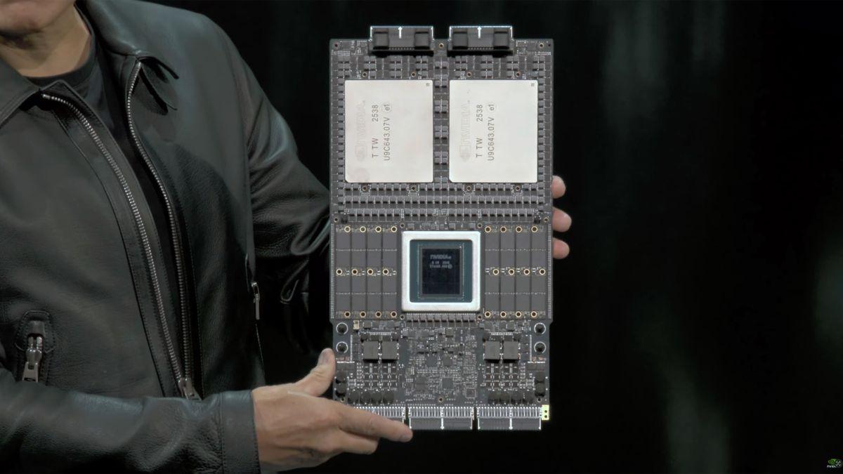
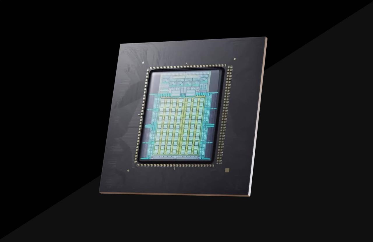
At its GTC keynote in DC on Tuesday, Nvidia unveiled its next-generation Vera Rubin Superchip, comprising two Rubin GPUs for AI and HPC as well as its custom 88-core Vera CPU. All three components will be in production this time next year, Nvidia says. "This is the next generation Rubin," said Jensen Huang, chief executive of Nvidia, at GTC. "While we are shipping GB300, we are preparing Rubin to be in production this time next year, maybe slightly earlier. [...] This is just an incredibly beautiful computer. So, this is amazing, this is 100 PetaFLOPS [of FP4 performance for AI]." Indeed, Nvidia's Superchips tend to look more like a motherboard (on an extremely thick PCB) rather than a 'chip' as they carry a general-purpose custom CPU and two high-performance compute GPUs for AI and HPC workloads. The Vera Rubin Superchip is not an exception, and the board carries Nvidia's next-generation 88-core Vera CPU surrounded by SOCAMM2 memory modules carrying LPDDR memory and two Rubin GPUs covered with two large rectangular aluminum heat spreaders. Markings on the Rubin GPU say that they were packaged in Taiwan on the 38 week of 2025, which is late September, something that proves that the company has been playing with the new processor for some time now. The size of the heatspreader is about the same size as the heatspreader of Blackwell processors, so we cannot figure out the exact size of GPU packaging or die sizes of compute chiplets. Meanwhile, the Vera CPU does not seem to be monolithic as it has visible internal seams, implying that we are dealing with a multi-chiplet design. A picture of the board that Nvidia demonstrated once again reveals that each Rubin GPU is comprised of two compute chiplets, eight HBM4 memory stacks, and one or two I/O chiplets. Interestingly, but this time around, Nvidia demonstrated the Vera CPU with a very distinct I/O chiplet located next to it. Also, the image shows green features coming from the I/O pads of the CPU die, the purpose of which is unknown. Perhaps, some of Vera's I/O capabilities are enabled by external chiplets that are located beneath the CPU itself. Of course, we are speculating, but there is definitely an intrigue with the Vera processor. Interestingly, the Vera Rubin Superchip board no longer has industry-standard slots for cabled connectors. Instead, there are two NVLink backplane connectors on top to connect GPUs to the NVLink switch, enabling scale-up scalability within a rack and three connectors on the bottom edge for power, PCIe, CXL, and so on. In general, Nvidia's Vera Rubin Superchip board looks quite baked, so expect the unit to ship sometime in late 2026 and get deployed by early 2027.
[3]
Nvidia showcases Vera Rubin AI "Superchip" with 88 CPU cores and 100 PetaFLOPS of FP4 compute
Serving tech enthusiasts for over 25 years. TechSpot means tech analysis and advice you can trust. What just happened? Nvidia has shifted its focus amid the AI boom from its gaming and professional GPU business to AI hardware design, driving its market value to nearly $5 trillion. The company has now unveiled its next-generation AI platform: the Vera Rubin "Superchip," purpose-built for high-intensity generative AI workloads. The new hardware was unveiled this week at Nvidia's GPU Technology Conference (GTC) in Washington by co-founder and CEO Jensen Huang. The Vera Rubin platform features a single "Vera" CPU with 88 custom Arm cores and 176 threads, alongside two "Rubin" GPUs, delivering up to 100 petaFLOPS of FP4 compute performance. Vera Rubin is Nvidia's third-generation LVLink 72 rack-scale computer, following the GB200 and GB300. The liquid-cooled system contains six trillion transistors and hosts 2 TB of low-latency SOCAMM2 memory. The base configuration delivers roughly 100 times the raw compute performance of the Volta-based DGX-1, Nvidia's first purpose-built platform for deep learning, which offered 170 teraflops of half-precision (FP16) peak performance. Vera Rubin will be offered in multiple configurations, including the NVL144 and NVL144 CPX. The NVL144 features two reticle-sized GPUs, delivering up to 3.6 exaflops of FP4 inference and 1.2 exaflops of FP8 training performance. The NVL144 CPX is rated at 8 exaflops - 7.5 times more powerful than Nvidia's current-generation GB300 NVL72 systems. For hyperscale data centers requiring even more processing power for larger model-context workloads, Nvidia will offer its custom Rubin Ultra NVL576 systems. Configured with four reticle-sized GPUs and up to 365 TB of high-speed memory, the NVL576 delivers up to 15 exaflops of FP4 inference and 5 exaflops of FP8 training performance - an 8× increase over the GB300. Each Rubin GPU comprises two compute chiplets and eight HBM4 memory stacks. The board also includes five NVLink backplane connectors - two at the top and three at the bottom. The top connectors are designed to link GPUs to the NVLink switch, while the bottom connectors handle power, PCIe, and CXL connectivity. Huang expects Rubin GPUs to enter mass production in the second half of 2026. NVL144 systems are slated to launch either later that year or in early 2027, while NVL576 systems will likely debut in the second half of 2027.
[4]
Nvidia's new six-trillion transistor Vera Rubin 'superchip' for AI makes the 92-billion transistor RTX 5090 gaming GPU look positively puny
Nvidia's ever-optimistic CEO, Jensen Huang, has revealed more details of the company's next-gen AI platform at the same GTC event where the company's quantum computing plans were outlined. He calls it the Vera Rubin "superchip" and claims it contains no fewer than six trillion transistors. Yup, six trillion. In very simple terms, that means the Vera Rubin superchip sports 60 times the number of transistors of an Nvidia RTX 5090 gaming GPU. And that is a completely bananas comparison. What's more, the Vera Rubin superchip is capable of 100 petaflops of raw compute. And that is exactly 100 times more compute than Nvidia claims for its neat little DGX Spark AI box. Oh, and it packs 88 custom Arm cores suporting 176 software threads for conventional CPU compute, too. On a side note, that Arm CPU bit (which alone is known as Vera) is interesting from a PC perspective as you might expect its custom designed CPU cores, which notably support multi-threading, could turn up in a PC processor in the future. Watch this space. At this point you may be wondering how any of this is possible. Six trillion transistors, 100 PF of compute, 88 CPU cores, all in one chip? OK, Vera Rubin is expected to upgrade to TSMC's latest N3 process node. But the N5-derived node that Nvidia currently uses for its GPUs tops out at a little over 100 billion transistors for a single, monolithic chip. N3 is more dense than N5, for sure. But not anything like enough to go from about 100 billion to six trillion transistors. Actually, it turns out that Vera Rubin isn't just more than one chip, it's more than one chip package. Huang held up an engineering sample of Vera Rubin and what's clear to see are the three main chip packages, one for the CPU and two GPU packages. In a later part of the presentation, it becomes clear that each GPU package actually contains two GPUs. So that's four GPUs total, plus the CPU. A close up on the Vera CPU package also reveals it to be a chiplet design, further elevating the overall transistor count headroom. That said, each Rubin AI GPU die is monolithic and described as reticle-sized, which means it's as big as TSMC's production process will allow. But even if you were generous and assumed that TSMC could squeeze 200 billion transistors into a single monolithic chip using N3, you'd need 30 such chips to get to that six trillion figure. Actually, Nvidia also revealed a "Rubin Ultra" GPU package with four Rubin GPU dies, so this stuff is just going to scale and scale. But, still, it's unclear how Nvidia is doing its transistor count. I'd have to assume that everything, including all the memory for the GPUs and CPU, plus the supporting chips on the Vera Rubin motherboard, is thrown in. However Nvidia is coming up with the numbers, the Vera Rubin AI board (as opposed to "chip" as Huang is calling it), is an unfathomably complex thing. Indeed, Huang says it's 100 times faster than the Nvidia equivalent product from nine years ago, the DGX One, which Huang says he delivered to what must then have been a nascent OpenAI. The rest, as they say, is history. And trillions and trillions of transistors. And trillions of dollars for Nvidia. For the record, Huang says Vera Rubin goes into production "this time next year, maybe even slightly earlier" and it probably won't be cheap. So get saving up.
[5]
NVIDIA Vera Rubin Superchip Unveiled at GTC 2025 - 88-Core Arm CPU and Dual Rubin GPUs
At the GTC event in Washington D.C., NVIDIA gave the world its first look at the new Vera Rubin Superchip system -- a massive leap in design for high-performance computing and AI workloads. This setup combines two Rubin GPUs with a single Vera CPU inside one package, forming what NVIDIA calls a "symbiotic" processor architecture. The Vera CPU packs 88 custom-built Arm-based cores with 176 threads, giving it serious muscle for data-heavy workloads. Together, the two Rubin GPUs deliver about 100 PetaFLOPS of FP4 performance -- that's 50 PetaFLOPS each -- and are aimed at large-scale AI training and inference tasks. Each Rubin GPU looks like a twin-chiplet design, using two giant dies of around 830 mm² apiece and eight HBM4 memory stacks. That adds up to roughly 288 GB of HBM4 per GPU, or 576 GB in total for the full Superchip. On top of that, the board also carries SOCAMM2 LPDDR5X memory modules, providing around 1.5 TB of extra low-latency system RAM per Vera CPU. NVLink has been upgraded to an incredible 1.8 TB/s bandwidth, allowing massive data flow between CPU and GPU -- essential for today's enormous AI models. NVIDIA built this system as the heart of its future NVL-class data center hardware. The smaller NVL144 configuration will use 144 GPUs to reach around 3.6 ExaFLOPS of FP4 inference performance and about 1.2 ExaFLOPS for FP8 training. That setup combines roughly 13 TB/s of memory bandwidth and 75 TB of system memory. For the biggest data centers, the upcoming Rubin Ultra NVL576 design scales even further, with total compute pushing close to 15 ExaFLOPS FP4 and hundreds of terabytes of fast memory. Production of the Vera Rubin Superchip is expected to begin in 2026, with wider rollout planned for 2027. Engineering samples are already being tested in labs, and early data suggests NVIDIA is taking a fully in-house approach with the Vera CPU instead of licensing Arm's Neoverse cores as it did with the Grace chips. Source: NVIDIA
[6]
Nvidia unveils the Vera Rubin AI Superchip, its most powerful system yet
The system features 88 custom ARM cores and 2 TB of low-latency memory for generative AI workloads. Nvidia co-founder and CEO Jensen Huang unveiled the Vera Rubin AI Superchip at the GPU Technology Conference in Washington, marking the company's shift to AI hardware amid the AI boom, boosting its market value to nearly $5 trillion. The Vera Rubin platform targets high-intensity generative AI workloads. It integrates a single Vera CPU equipped with 88 custom ARM cores that support 176 threads. This CPU pairs with two Rubin GPUs to achieve up to 100 petaFLOPS of FP4 compute performance. As Nvidia's third-generation NVLink 72 rack-scale computer, Vera Rubin succeeds the GB200 and GB300 models. The system employs liquid cooling and incorporates six trillion transistors. It also includes 2 TB of low-latency SOCAMM2 memory to handle demanding AI processing tasks efficiently. In its base configuration, Vera Rubin provides roughly 100 times the raw compute performance compared to the Volta-based DGX-1. That earlier platform, Nvidia's initial deep learning system, delivered 170 teraflops of FP16 peak performance. This substantial increase underscores the evolution in computational capacity for AI applications over the years. Nvidia plans to release Vera Rubin in various configurations to meet diverse needs. The NVL144 setup includes two reticle-sized GPUs, which enable up to 3.6 exaflops of FP4 inference and 1.2 exaflops of FP8 training performance. For enhanced capabilities, the NVL144 CPX configuration reaches 8 exaflops, representing 7.5 times the power of the current-generation GB300 NVL72 systems. To address requirements in hyperscale data centers for processing larger model-context workloads, Nvidia introduces the Rubin Ultra NVL576 system. This variant uses four reticle-sized GPUs along with up to 365 TB of high-speed memory. It delivers up to 15 exaflops of FP4 inference and 5 exaflops of FP8 training performance, which amounts to an 8 times increase over the GB300. Each Rubin GPU consists of two compute chiplets and eight HBM4 memory stacks, optimizing data throughput and computation. The GPU board features five NVLink backplane connectors. Two connectors at the top connect the GPUs to the NVLink switch for high-speed interconnectivity. The three bottom connectors manage power delivery, PCIe interface, and CXL connectivity to support integration within broader systems. Huang anticipates that Rubin GPUs will enter mass production during the second half of 2026. The NVL144 systems are scheduled for launch later in 2026 or early 2027. Meanwhile, the NVL576 systems are expected to become available in the second half of 2027, aligning with Nvidia's roadmap for advancing AI infrastructure.
[7]
NVIDIA Shows Next-Gen Vera Rubin Superchip For The First Time, Two Massive GPUs Primed For Production Next Year
NVIDIA has shown off its next-gen Vera Rubin Superchip for the first time at GTC in Washington, primed to spark the next wave of AI. At GTC October 2025, NVIDIA's CEO Jensen Huang showcased the next-gen Vera Rubin Superchip. This is the first time that we are seeing an actual sample of the motherboard, or Superchip as NVIDIA loves to call it, featuring the Vera CPU and two massive Rubin GPUs. The motherboard also hosts lots of LPDDR system memory, which will be combined with HBM4 memory featured on the Rubin GPUs. In terms of specifications, the NVIDIA Vera Rubin NVL144 platform will utilize two new chips. The Rubin GPU will make use of two Reticle-sized chips, with up to 50 PFLOPs of FP4 performance and 288 GB of next-gen HBM4 memory. These chips will be equipped alongside an 88-core Vera CPU with a custom Arm architecture, 176 threads, and up to 1.8 TB/s of NVLINK-C2C interconnect. In terms of performance scaling, the NVIDIA Vera Rubin NVL144 platform will feature 3.6 Exaflops of FP4 inference and 1.2 Exaflops of FP8 Training capabilities, a 3.3x increase over GB300 NVL72, 13 TB/s of HBM4 memory with 75 TB of fast memory, a 60% uplift over GB300 and 2x the NVLINK and CX9 capabilities, rated at up to 260 TB/s and 28.8 TB/s, respectively. The second platform will be arriving in the second half of 2027 and will be called Rubin Ultra. This platform will scale the NVL system from 144 to 576. The architecture for the CPU remains the same, but the Rubin Ultra GPU will feature four reticle-sized chips, offering up to 100 PFLOPS of FP4 and a total HBM4e capacity of 1 TB scattered across 16 HBM sites. In terms of performance scaling, the NVIDIA Rubin Ultra NVL576 platform will feature 15 Exaflops of FP4 inference and 5 Exaflops of FP8 Training capabilities, a 14x increase over GB300 NVL72, 4.6 PB/s of HBM4 memory with 365 TB of fast memory, a 8x uplift over GB300 and 12x the NVLINK and 8x the CX9 capabilities, rated at up to 1.5 PB/s and 115.2 TB/s, respectively.
Share
Share
Copy Link
Nvidia reveals its next-generation Vera Rubin Superchip featuring 88-core Vera CPU and dual Rubin GPUs, delivering 100 PetaFLOPS of AI compute performance. The platform represents a massive leap in AI hardware capabilities, targeting production in 2026.
Revolutionary AI Hardware Platform
Nvidia has unveiled its most ambitious AI hardware platform to date: the Vera Rubin Superchip, a six-trillion transistor system that promises to redefine the boundaries of artificial intelligence computing. CEO Jensen Huang presented the groundbreaking technology at the company's GPU Technology Conference in Washington D.C., describing it as "an incredibly beautiful computer" that delivers 100 PetaFLOPS of FP4 performance for AI workloads
1
.
Source: PC Magazine
The Vera Rubin platform represents a fundamental shift in AI hardware design, combining an 88-core Vera CPU with dual Rubin GPUs on a single board. This "symbiotic" processor architecture is built using next-generation designs that more than double the CPU core count compared to Nvidia's current-generation GB200 Grace Blackwell flagship
2
.
Source: Tom's Hardware
Technical Specifications and Architecture
The Vera Rubin Superchip showcases remarkable engineering complexity, featuring three main chip packages mounted on an extremely thick PCB that resembles a motherboard more than a traditional chip. The 88-core Vera CPU utilizes custom Arm-based cores supporting 176 software threads, representing a significant departure from standard processor designs
3
.Each Rubin GPU comprises two compute chiplets and eight HBM4 memory stacks, providing 288GB of HBM4 memory per GPU for a total of 576GB across both GPUs. The system also incorporates SOCAMM2 LPDDR5X memory modules, delivering approximately 1.5TB of additional low-latency system RAM. Enhanced NVLink-C2C connectivity provides an unprecedented 1.8TB/s bandwidth, enabling massive data flow between CPU and GPU components essential for processing today's enormous AI models
5
.
Source: Guru3D
Performance Capabilities and Configurations
The performance specifications of Vera Rubin are staggering by current standards. The base configuration delivers roughly 100 times the raw compute performance of Nvidia's original DGX-1 platform, which offered 170 teraflops of half-precision performance when it launched as the company's first purpose-built deep learning system
3
.Nvidia plans multiple configurations to serve different market segments. The NVL144 system will offer 3.6 ExaFLOPS of FP4 inference performance and 1.2 ExaFLOPS of FP8 training performance, representing approximately 3.3 times faster performance than the current GB300 NVL72 platform. For hyperscale data centers requiring even greater processing power, the Rubin Ultra NVL576 configuration will debut in 2027 with four reticle-sized GPUs, up to 365TB of high-speed memory, and performance reaching 15 ExaFLOPS for FP4 inference and 5 ExaFLOPS for FP8 training
1
.Related Stories
Manufacturing and Market Impact
The six-trillion transistor count represents a remarkable achievement in semiconductor manufacturing, made possible through advanced chiplet design and TSMC's latest N3 process node. Each Rubin GPU die is described as reticle-sized, meaning it utilizes the maximum area that TSMC's production process allows. The complexity extends beyond the main processors to include all supporting memory and chipsets integrated onto the Vera Rubin motherboard
4
.Engineering samples are already undergoing testing in laboratories, with markings indicating GPU packaging completed in Taiwan during late September 2025. This suggests Nvidia has been developing and refining the technology for considerable time. The company expects to begin mass production in the second half of 2026, with broader deployment anticipated in early 2027
2
.References
Summarized by
Navi
[1]
[2]
[3]
Related Stories
Nvidia ships first Vera Rubin AI chips to customers, promising 10x efficiency gains over Blackwell
25 Feb 2026•Technology
Nvidia Vera Rubin architecture slashes AI costs by 10x with advanced networking at its core
06 Jan 2026•Technology
NVIDIA Unveils Next-Gen AI Powerhouses: Rubin and Rubin Ultra GPUs with Vera CPUs
19 Mar 2025•Technology

Recent Highlights


Recent Highlights
Today's Top Stories


Your Daily Dose of Curated AI News
Don’t drown in AI news. We cut through the noise - filtering, ranking and summarizing the most important AI news, breakthroughs and research daily. Spend less time searching for the latest in AI and get straight to action.