SK Hynix Leads the Charge in HBM4 Development, Promising Unprecedented Performance for AI
6 Sources
6 Sources
[1]
SK hynix completes development of HBM4 -- 2,048-bit interface and 10 GT/s speeds promised
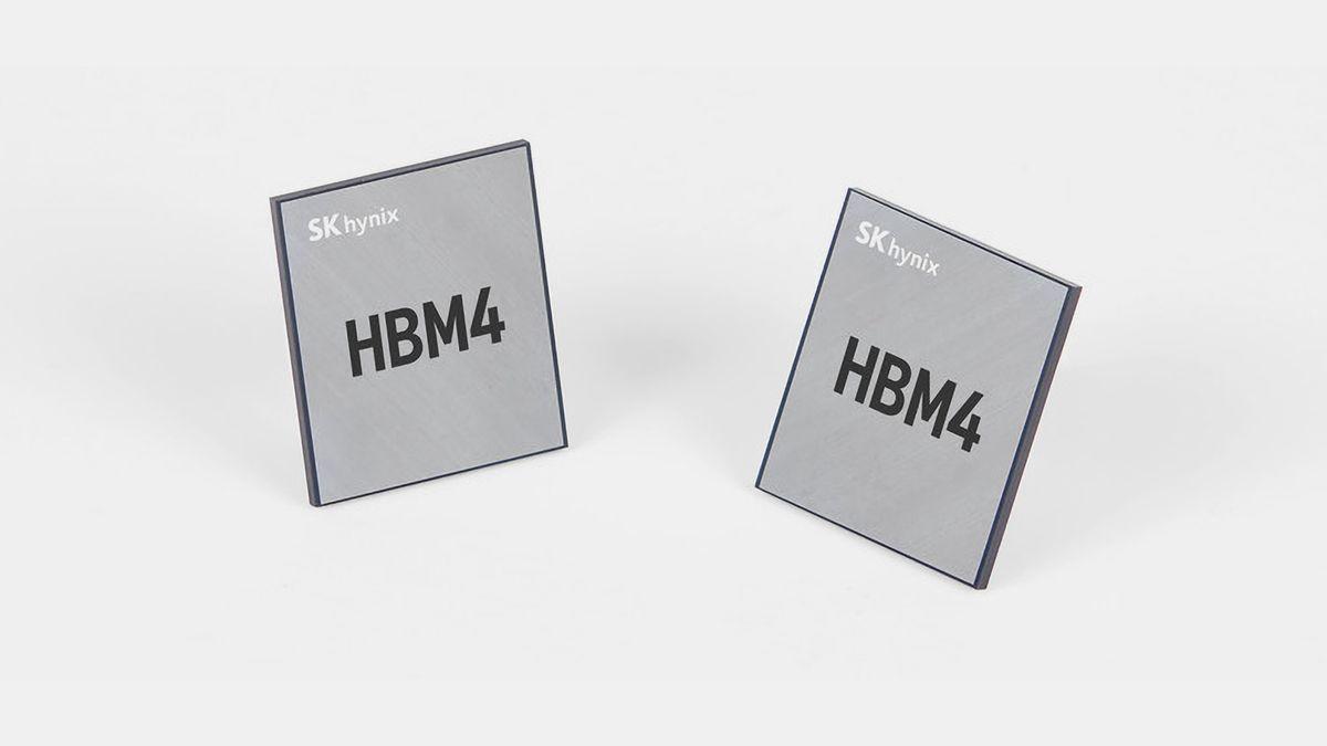
SK hynix has completed development of its HBM4 memory and prepared it for high-volume manufacturing of memory stacks, the company said on Friday. HBM4 stacks from SK hynix go beyond specifications set by JEDEC by 25% in terms of performance, though it remains to be seen whether producers of next-generation AI accelerators -- such as AMD, Broadcom, or Nvidia -- will use that potential on their 2026 products. SK hynix's HBM4 memory stacks feature a 2,048-bit I/O, doubling the width of the HBM interface for the first time since 2015, and a 10 GT/s data transfer rate, which is 25% higher compared to the official JEDEC standard (more on this later). The company's HBM4 memory stacks use specially designed DRAM dies built using proven 1b-nm (5th Generation 10nm-class) process technology that combines decent performance efficiency with node maturity (i.e., low defect density and variability). For its HBM4 modules, SK hynix continues to use its proven Advanced Mass Reflow Molded Underfill (MR-MUF) method. In this process, multiple memory chips are placed on a base substrate and bonded together in a single reflow step. Right after that, spaces between the stacked DRAM layers, base die, and substrate are filled with a mold material to secure and protect the structure. Advanced MR-MUF enables the company to keep the height of its 12-Hi HBM stacks within specification and improve heat dissipation of power-hungry memory modules. "Completion of HBM4 development will be a new milestone for the industry," Joohwan Cho, Head of HBM Development at SK hynix, who has led the development, said. "By supplying the product that meets customer needs in performance, power efficiency and reliability in timely manner, the company will fulfill time to market and maintain competitive position." Unfortunately, SK hynix does not disclose either how many DRAM layers its HBM4 devices use, or their capacity, though we are likely talking about 12-Hi 36 GB devices that will be used for Nvidia's Rubin data center GPUs, but we are speculating. The company also does not disclose whether its initial HBM4 stacks use 12FFC+ (12nm-class) or N5 (5nm-class) base logic dies produced by TSMC. Arguably, the most interesting part of SK hynix's announcement is the fact that it decided to go beyond JEDEC's specification and certify its HBM4 stacks for a 10 GT/s data transfer rate, up from the 8 GT/s set by the standard. The company is not alone in going beyond JEDEC spec with HBM4: Micron is currently sampling HBM4 devices with a 9.2 GT/s data transfer rate, whereas Rambus has an HBM4 memory controller capable of 10 GT/s speed. While extra performance may be used by actual chip developers at some point, most developers apparently want to have some reserve for added piece of mind, according to an insight shared by Rambus a few years ago. SK hynix says that it is ready to mass produce its HBM4 stacks, though it does not disclose when it plans to kick off volume production of HBM4. "We are unveiling the establishment of the world's first mass production system of HBM4," said Justin Kim, President & Head of AI Infra at SK hynix. "HBM4, a symbolic turning point beyond the AI infrastructure limitations, will be a core product for overcoming technological challenges. We will grow into a full-stack AI memory provider by supplying memory products with the best quality and diverse performance required for the AI era in a timely manner."
[2]
SK Hynix says its HBM4 is ready for mass production
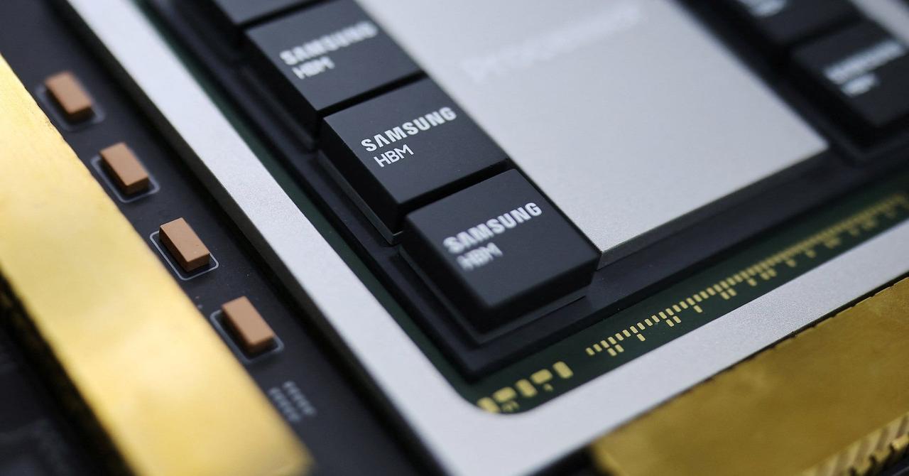
Top AI chipmakers count on faster, denser, more efficient memory to boost training AMD and Nvidia have already announced their next-gen datacenter GPUs will make the leap to HBM4, and if SK Hynix has its way, it'll be the one supplying the bulk of it. On Friday, the South Korean memory giant announced that it had wrapped HBM4 development and was preparing to begin producing the chips in high volumes. The news sent SK's share price on a 7 percent rally and for good reason. High Bandwidth Memory (HBM) has become an essential component in high-end AI accelerators from the likes of Nvidia, AMD, and others. Both Nvidia's Rubin and AMD's Instinct MI400 families of GPUs, pre-announced earlier this year, rely on memory vendors having a ready supply of HBM4 in time for their debut in 2026. The transition comes as the GPU slingers run up against the limits of existing HBM technologies, which currently top out at around 36 GB of capacity and about 1 TB/s of bandwidth per module, giving chips like Nvidia's B300 or AMD's MI355X about 8 TB/s of aggregate memory bandwidth. With the move to HBM4, we'll see bandwidth jump considerably. At GTC in March, Nvidia revealed its Rubin GPUs would pack 288 GB of HBM4 and achieve 13 TB/s of aggregate bandwidth. AMD aims to cram even greater quantities of memory onto its upcoming MI400-series GPUs, which will power its first rack-scale system called Helios. As we learned at AMD's Advancing AI event in June, the parts will pack up to 432 GB of HBM with an aggregate bandwidth approaching 20 TB/s. SK Hynix says that it has effectively doubled the bandwidth of its HBM by increasing the number of I/O terminals to 2,048, twice what we saw on HBM3e. This, it argues, has also boosted energy efficiency by more than 40 percent. While the DRAM typically in servers isn't usually a major energy consumer, HBM is. With the shift from 24 GB on AMD's MI300X to the 36 GB modules found on the MI325, power consumption jumped from 250 W to roughly a kilowatt per GPU. SK Hynix says that, along with more I/O terminals and improved efficiency, its chips have also managed to exceed the JEDEC standard for HBM4, achieving 10 Gb/s operating speed. Which of the three big HBM vendors will end up supplying these chips remains to be seen. While SK Hynix has won the majority of Nvidia's HBM business over the past few years, Samsung and Micron are also working to bring HBM4 to the market. Micron began sampling 36 GB 12-high HBM4 stacks to customers in June. Much like with SK Hynix, the stacks are using a 2048-bit interface and will achieve roughly twice the bandwidth of the HBM3e modules available today. The American memory vendor expects to ramp production of the stacks sometime next year. Meanwhile, for Samsung, HBM4 presents a new opportunity to win over Nvidia's business. The vendor has reportedly struggled to get its HBM3e stacks validated for use in the GPU giant's Blackwell accelerators. ®
[3]
SK Hynix says readying HBM4 production after completing internal certification
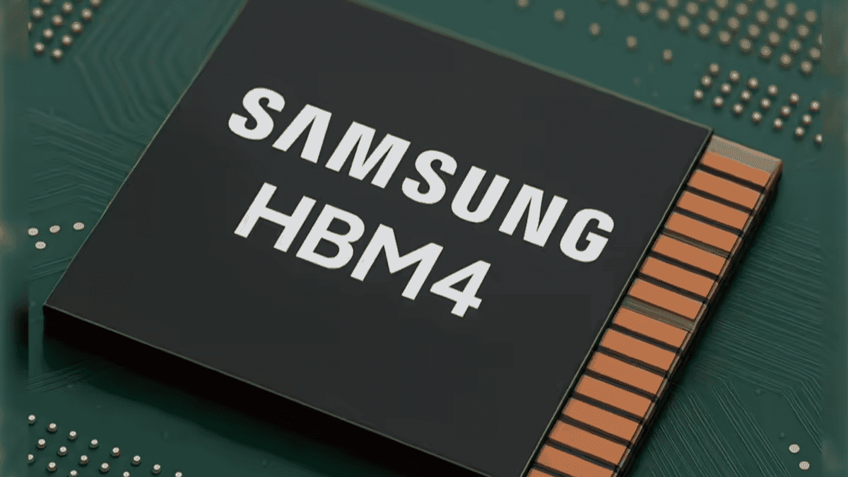
SEOUL, Sept 12 (Reuters) - South Korea's SK Hynix (000660.KS), opens new tab said on Friday it has completed its internal certification process for next generation high-bandwidth memory 4(HBM4) chips and established a production system for customers. In March, the South Korean chipmaker, a key supplier to AI giant Nvidia (NVDA.O), opens new tab, said it had shipped its HBM4 12-layer chip samples to customers, adding that the company aims to complete preparations for mass production of 12-layer HBM4 products within the second half of this year. HBM - a type of dynamic random access memory or DRAM standard first produced in 2013 - involves stacking chips vertically to save space and reduce power consumption, helping to process the large volumes of data generated by complex AI applications. SK Hynix shares hit a record high in morning trade, rising as much as 7.3%, outpacing the benchmark KOSPI's 1.2% rise, as analysts cited the company's HBM4 chip production plans. Kim Sunwoo, a senior analyst at Meritz Securities, projected that SK Hynix's HBM market share will remain in the low 60% range in 2026, supported by early HBM4 supply to key customers and the resulting first-mover advantage. SK Hynix is currently the main HBM supplier to Nvidia, although Samsung Electronics (005930.KS), opens new tab and Micron (MU.O), opens new tab supply it with smaller volumes. An SK Hynix executive told Reuters in an interview last month that because of technological changes in how SK Hynix and rivals such as Micron and Samsung build next-generation HBM4, their products include a customer-specific logic die, or "base die", that helps manage the memory. That means it is no longer possible to easily replace a rival's memory product with a nearly identical chip or product. Samsung said in July that it had provided samples of its HBM4 chips to customers, with a plan to supply them next year. Reporting by Heekyong Yang and Jihoon Lee; Editing by Ed Davies Our Standards: The Thomson Reuters Trust Principles., opens new tab
[4]
SK Hynix completes HBM4 development, aims to mass produce memory for AI workloads
HBM4 doubles connections and improves efficiency by 40 percent South Korean memory giant SK Hynix says it has completed development work on HBM4 and is now preparing the technology for mass production. This puts it ahead of rivals Samsung and Micron, who are still developing their own versions. The chips are expected to feature in Nvidia's next-generation Rubin AI processors, and will play an important role in powering future artificial intelligence workloads. Joohwan Cho, Head of HBM Development at SK Hynix, said: "Completion of HBM4 development will be a new milestone for the industry. By supplying the product that meets customer needs in performance, power efficiency and reliability in timely manner, the company will fulfill time to market and maintain competitive position." High Bandwidth Memory, or HBM, stacks layers of DRAM vertically to accelerate data transfer. Demand for high bandwidth memory has risen with the surge in AI workloads, and energy efficiency has become a pressing concern for data center operators. HBM4 doubles the number of I/O connections compared with the previous generation and improves power efficiency by more than 40%. The Korean memory maker says this translates into higher throughput and lower energy use in data centers, with service performance gains of up to 69%. HBM4 surpasses the JEDEC industry standard operating speed of 8Gbps by running above 10Gbps. SK Hynix adopted its advanced MR-MUF process for stacking chips, which improves heat dissipation and stability, along with the 1bnm process technology to help minimize manufacturing risk. Justin Kim, President and Head of AI Infra at SK Hynix, said: "We are unveiling the establishment of the world's first mass production system of HBM4. HBM4, a symbolic turning point beyond the AI infrastructure limitations, will be a core product for overcoming technological challenges. We will grow into a full-stack AI memory provider by supplying memory products with the best quality and diverse performance required for the AI era in a timely manner."
[5]
SK hynix finishes HBM4 development, ready for mass production: 10Gbps per pin, above 8Gbps spec
TL;DR: SK hynix has completed development and prepared mass production of its next-gen HBM4 memory, delivering industry-leading 10Gbps speeds, 40% improved power efficiency, and doubled bandwidth. Designed for ultra-high-performance AI and data centers, HBM4 promises up to 69% AI service performance gains and reduced power costs. SK hynix has confirmed it has successfully completed the development and finished preparation of its next-gen HBM4 memory, ready for ultra-high-performance AI, and will enter mass production for the world's first time. The South Korean firm has said that it's successfully completed development and based on this technological achievement, SK hynix has prepared HBM4 mass production to "lead the AI era". We will see SK hynix HBM4 memory inside of next-gen AI chips like NVIDIA's upcoming Rubin AI GPUs in 2026. Joohwan Cho, Head of HBM Development at SK hynix, who has led the development, said: "Completion of HBM4 development will be a new milestone for the industry. By supplying the product that meets customer needs in performance, power efficiency and reliability in a timely manner, the company will fulfill time to market and maintain competitive position". On a new post on its website, SK hynix says that with the recent dramatic increase in AI demand and data processing, the needs for high bandwidth memory (HBM) for faster system speed are "surging". Not only that, but securing memory power efficiency has emerged as a key requirement as power consumption for data center operations has increased. SK hynix has far exceeded the JEDEC standard operating speed of 8Gbps for HBM4, pushing up into 10Gbps operating speeds for its HBM4 memory. HBM4 has the industry's best data processing speed and power efficiency, doubling the bandwidth through the adoption of 2048 I/O terminals over the previous-gen HBM3 standard, and power efficiency has climbed by over 40%. SK hynix expects AI service performance improvements by up to 69% when HBM4 is used, which will "lead to solving data bottlenecks and significantly reduce data center power costs".
[6]
SK hynix Inc. Completes First HBM4 Development and Readies Mass Production
SK hynix Inc. announced that it has completed development and finished preparation of HBM4, a next generation memory product for ultra-high performance AI, mass production for the world's first time. HBM(High Bandwidth Memory): This high-value, high-performance memory vertically interconnects multiple DRAM chips and dramatically increases data processing speed in comparison to conventional DRAM products. There are six generations of HBM, starting with the original HBM which was followed by HBM2, HBM2E, HBM3, HBM3E, and HBM4. SK hynix said that the company has successfully completed development and based on this technological achievement, the company has prepared HBM4 mass production to lead the AI era. Through this momentum, the company has once again proven the AI memory leadership in the global market. With recent dramatic increase in AI demand and data processing, the needs for high bandwidth memory for faster system speed are surging. In addition, securing memory power efficiency has emerged as a key requirement for customers as power consumption for data center operation has increased. SK hynix expects HBM4, with increased bandwidth and power efficiency, to be the optimal solution to meet customers' needs. Bandwidth: In HBM products, bandwidth refers to the total data capacity that one HBM package can process per second. HBM4, of which mass production system has been readied, has the industry's best data processing speed and power efficiency with the bandwidth doubled through adoption of 2,048 I/O terminals, double from the previous generation, and power efficiency improved by more than 40%. The company expects to improve AI service performance by up to 69% when the product is applied, which will lead to solve data bottleneck and significantly reduce data center power costs. The company has far exceeded the JEDEC standard operating speed(8Gbps) by implementing over 10Gbps(Gigabit per second) operating speed in HBM4. JEDEC(Joint Electron Device Engineering Council): A standardization body that is the global leader in developing open standards and publications for the microelectronics industry. In addition, the company adopted the Advanced MR-MUF process in HBM4, which has been proven to be reliable in the market, and the 1bnm process, or the fifth-generation of the 10-nanometer technology, to minimize the risk in mass production. MR-MUF(Mass Reflow Molded Underfill): The process of stacking semiconductor chips, injecting liquid protective materials between them to protect the circuit between chips, and hardening them. The process has proved to be more efficient and effective for heat dissipation, compared with the method of laying film-type materials for each chip stack. SK hynix's advanced MR-MUF technology is critical to securing a stable HBM mass production as it provides good warpage control and reduces the pressure on the chips being stacked.
Share
Share
Copy Link
SK Hynix announces completion of HBM4 memory development, ready for mass production. The new memory technology offers significant improvements in bandwidth, speed, and energy efficiency, potentially revolutionizing AI and data center operations.
SK Hynix Pioneers HBM4 Technology
SK Hynix, the South Korean memory giant, has announced a significant breakthrough in the development of High Bandwidth Memory (HBM) technology. The company has successfully completed the development of HBM4 and is now preparing for mass production, potentially giving it a competitive edge over rivals Samsung and Micron
1
3
.Technical Advancements and Performance Gains
HBM4 represents a substantial leap forward in memory technology, particularly for AI and data center applications. Key improvements include:
- Doubled I/O interface: HBM4 features a 2,048-bit I/O, twice the width of previous generations
1
. - Increased speed: SK Hynix's HBM4 achieves a 10 GT/s data transfer rate, surpassing the JEDEC standard of 8 GT/s by 25%
1
5
. - Enhanced efficiency: Power efficiency has improved by over 40% compared to previous generations
4
.
These advancements are expected to result in up to 69% improvement in AI service performance while significantly reducing data center power costs
5
.Manufacturing and Design Innovations
SK Hynix employs several cutting-edge techniques in the production of HBM4:
- Advanced process node: The DRAM dies are built using 1b-nm (5th Generation 10nm-class) process technology
1
. - Stacking method: The company utilizes its proven Advanced Mass Reflow Molded Underfill (MR-MUF) method for chip stacking
1
. - Heat management: The MR-MUF process also improves heat dissipation in these power-hungry memory modules
1
.
Related Stories
Market Implications and Competition
The completion of HBM4 development positions SK Hynix favorably in the competitive memory market:
- First-mover advantage: SK Hynix claims to have established the world's first mass production system for HBM4
3
. - Market share projection: Analysts predict SK Hynix could maintain a low 60% range market share in HBM by 2026
3
. - Competition: Samsung and Micron are also developing HBM4 but appear to be trailing SK Hynix in terms of readiness for mass production
2
3
.
Future Applications and Industry Impact
HBM4 is set to play a crucial role in next-generation AI and data center technologies:
- AI accelerators: Both Nvidia and AMD have announced plans to use HBM4 in their upcoming data center GPUs, including Nvidia's Rubin and AMD's Instinct MI400 series
2
. - Bandwidth improvements: Next-gen GPUs are expected to achieve aggregate bandwidths of 13-20 TB/s, a significant increase from current capabilities
2
. - Memory capacity: Future GPUs may incorporate up to 432 GB of HBM4, enabling more complex AI workloads
2
.
As the AI industry continues to grow rapidly, the demand for high-performance memory solutions like HBM4 is expected to surge, potentially reshaping the competitive landscape of the memory market and accelerating advancements in AI technologies.
References
Summarized by
Navi
[1]
[2]
Related Stories
SK hynix Leads the Charge in Next-Gen AI Memory with World's First 12-Layer HBM4 Samples
19 Mar 2025•Technology

Next-Gen HBM Memory Race Heats Up: SK Hynix and Micron Prepare for HBM3E and HBM4 Production
22 Dec 2024•Technology

Samsung HBM4 nears Nvidia approval as rivalry with SK Hynix intensifies for Rubin AI platform
26 Jan 2026•Technology
Recent Highlights
1
Apple Plans Major Siri AI Overhaul in iOS 27 With Third-Party Chatbot Integration
Technology

2
OpenAI shuts down Sora after six months, ending Disney's $1 billion licensing partnership
Technology

3
AI chatbots validate you too much, making you less kind to others, Stanford study reveals
Science and Research

Recent Highlights
Today's Top Stories


Your Daily Dose of Curated AI News
Don’t drown in AI news. We cut through the noise - filtering, ranking and summarizing the most important AI news, breakthroughs and research daily. Spend less time searching for the latest in AI and get straight to action.