Intel partners with SoftBank to develop Z-Angle Memory that promises triple HBM capacity
8 Sources
8 Sources
[1]
Intel is co-developing new Z-Angle Memory to compete with HBM used in AI data centers -- vertically-stacked memory touts 2 to 3x more capacity, greater bandwidth, and half the power consumption
Intel and a SoftBank subsidiary, Saimemory, have signed a new collaborative agreement to advance the development and manufacture of a new type of vertical-stacked memory known as Z-Angle Memory, or ZAM. This next-generation memory is designed to compete against High Bandwidth Memory (HBM) used in the latest AI data centers, but offers higher capacity, greater bandwidth, and lower power consumption. Although owned by Softbank, Saimemory was a joint development between Intel and Softbank. The two companies started building a prototype of this new memory standard in mid-2025, leveraging Intel's packaging technologies and key Japanese patents. The move brings Intel back into the memory market for the first time since the 1980s. It's also the first time a Japanese company has attempted to produce cutting-edge memory in decades. Japan was a major memory manufacturing region in the '80s, but the rise of Korean and Taiwanese manufacturing saw it fall out of favor. As the world scrambles for more memory, both Softbank and Intel see a clear opportunity to provide it. ZAM is designed to offer two to three times the capacity of HBM, operating at as little as half the power, while being up to 60% cheaper to produce, as reported by Nikkei. Saimemory will try to hit these lofty goals by vertically stacking more DRAM and using Intel's Embedded Multi-Die Interconnect Bridge (EMIB) to reduce latency between the individual chips. ZAM is built on the foundational work Intel completed as part of the Advanced Memory Technology R&D program, managed by the U.S. Department of Energy and National Nuclear Security Administration through the Sandia National Laboratory. They recognized that HBM has impressive bandwidth, but trades that for lower capacity and weaker power efficiency. Using Intel's new bonding techniques and novel DRAM stacking techniques allows for all the benefits of HBM, without those traditional downsides. "Intel's Next Generation DRAM Bonding (NGDB) initiative has demonstrated a novel memory architecture and revolutionary assembly methodology that significantly increases DRAM performance, reduces power consumption, and optimizes memory costs," said Dr. Joshua Fryman, Intel Fellow and CTO of Intel Government Technologies. "Standard memory architectures aren't meeting AI needs, so NGDB defined a whole new approach to accelerate us through the next decade." In developing the NGDB for ZAM, Intel and Sandia had to design a new stacking approach and a different way of organizing the DRAM chips. Early prototypes confirmed it was possible to increase capacity through new stacking techniques, while recent developments have demonstrated that the necessary high performance is there. That's why Intel and partners are now able to move forward with developing the first real prototypes of Z-Angle memory. Gwen Voskuilen, principal member of technical staff at Sandia, said, "This is an exciting technology that we anticipate will lead to a wider adoption of higher bandwidth memories in systems that are currently unable to take advantage of high bandwidth memory due to its limited capacity and power constraints." This venture isn't designed to suddenly bring new DDR5 or HBM production online, though. It's looking beyond what's currently available to data center builders and hoping to provide what they might need next. Saimemory is slated to produce its first ZAM prototype sometime in 2027, with plans to develop a mass production line for the new memory by 2029. Already, other firms are backing the project, showcasing its impact and interest beyond the initial parties to the venture. Other companies cooperating on the design, development, and manufacture of ZAM include Japanese IT hardware and services firm Fujitsu; the recent Micron acquisition, PowerChip Semiconductor Manufacturing; Shinko Electric Industries; and the University of Tokyo. The various Japanese institutions involved highlight the importance of this venture to Softbank. In its release, it said, "SAIMEMORY's development of next-generation memory technologies represents one of SoftBank's key initiatives to support next-generation social infrastructure." "By collaborating with Intel and other technology partners and research institutions in Japan and abroad, SoftBank will contribute to the creation of advanced, homegrown semiconductor technologies, and to the strengthening of Japan's global competitiveness." Alongside potentially rebuilding Japan as a key player in the memory industry, Softbank appears to see key technologies like next-generation memory as a core component of building aspects of the future that go beyond the raw hardware itself. In the same way that access to memory, silicon, and rare earth materials are increasingly considered an important asset for strategic defence, there's an argument to be made that they're also keystones in developing the components for social change in the decades to come, and the partnerships that will enable it. Intel and Softbank want to be a part of powering that.
[2]
SoftBank subsidiary to work with Intel on next-gen memory for AI
Saimemory, a subsidiary of multinational investment giant SoftBank, has signed a collaboration agreement with American chipmaker Intel Corp. to advance the commercialization of next-generation memory technology, the companies announced Tuesday. The partnership focuses on next-generation memory technologies that can support the growing demands of artificial intelligence and high-performance computing. The effort is currently known as the "Z-Angle Memory program," or ZAM. Prototypes are expected by the fiscal year ending March 31, 2028, with commercialization targeted for fiscal 2029, according to a SoftBank press release. Shares of SoftBank rose 3.13%, while Intel stock rose 5% in overnight trading on Robinhood following the announcement.
[3]
Intel is helping develop a new type of DRAM aimed at AI
This innovation builds on Intel's existing Foveros chip stacking technology and aims to reduce power consumption while meeting growing AI memory demands. Intel began as a memory supplier. The PC industry faces its most dire memory crunch in years, if not decades. So it makes sense for Intel to move back into PC memory, right? Sort of. Intel said this week that it is indeed working on a new memory technology, called Z-Angle Memory, or ZAM, with a Softbank-backed startup called Saimemory. It's not so much a new type of memory, but rather a new way of building memory, and one that should be familiar to Intel watchers. As the name suggests, ZAM is tied to "Z height," the way in which the thickness of various objects are described in the tech world. ZAM is a way to stack RAM on top of one another, increasing the available memory density for anything that needs DRAM, presumably from laptops to servers. The goal is to reduce power consumption and increase the amount of memory in a given volume, via what Intel calls Next-Generation DRAM Bonding, or NGDB. It also could be used as a high-bandwidth alternative to HBM, or high-bandwidth memory, which AMD began using in Radeon GPU chips beginning in 2015. High-speed memory is a critical building block of AI servers, too. Although Intel hasn't described in detail what NGDB can do, the company developed what's known as the Foveros technology, first announcing it in 2018. Foveros took Intel's EMIB technology and extended it vertically, allowing the company to stack logic chips on top of one another, or mount memory over logic as well. Now, Intel is mounting memory over memory in the new venture. Saimemory's contribution builds on foundational work supported by the Advanced Memory Technology (AMT) R&D Program, managed by the U.S. Department of Energy and National Nuclear Security Administration through the Sandia National Laboratory, Lawrence Livermore National Laboratory, and Los Alamos National Laboratory, the companies said in a press release. Saimemory will commercialize (sell) the product, while Intel will provide the technology. The company's manufacturing operations will begin this quarter, and prototypes are scheduled for 2027. The roadmap calls for ZAM to actually begin selling in 2030. Intel was founded in 1968 as a memory company, making SRAM and DRAM. Though it created the first microprocessor, the 4004, the company sold DRAM through the 1970s before pivoting to become a microprocessor supplier. With AI hyperscalers snapping up as much memory and storage as they can, however, knowing how to use whatever memory is available as effectively as possible might not be such a bad idea. After all, the great memory shortage could last for years.
[4]
Intel teams with SoftBank on next-gen ZAM memory, prototypes to compete against HBM in 2028
TL;DR: Intel partners with SoftBank's SAIMEMORY to advance next-generation DRAM bonding technology using Z-Angle Memory (ZAM), enabling higher capacity, lower power consumption, and improved performance for AI data centers. This innovation aims to revolutionize memory architecture, surpassing standard DRAM limits and enhancing large-scale AI processing efficiency. Intel is re-entering the memory business, teaming with Japan's SoftBank on a next-generation DRAM bonding technology. Intel's Next-Generation DRAM Bonding (NGDB) initiative was completed under the Advanced Memory Technology (AMT) program that was managed by the U.S. Department of Energy and National Nuclear Security Administration through the Sandia National Laboratory, Lawrence Livermore National Laboratory and Los Alamos National Laboratory... some advanced tech then, eh? The use of ZAM next-generation memory technology allows SoftBank's subsidiary, SAIMEMORY, to sign a collaborative agreement with Intel to advance the commercialization of Z-Angle Memory (ZAM), a next-generation memory technology. SoftBank's press release explains: "By utilizing ZAM next-generation memory technology, SAIMEMORY and Intel will work together to enable high-capacity and high-bandwidth data processing, enhanced processing performance and reduced power consumption in data centers and other environments that require the training and inference of large-scale AI models". Intel officials explained their next-gen DRAM bonding technology: "Standard memory architectures cannot meet the needs of artificial intelligence. NGDB defines a completely new approach that will accelerate our move into the next decade. We are rethinking how DRAM is organized to fundamentally advance computer system architecture, aiming to achieve orders-of-magnitude performance improvements and incorporate innovation into industry standards". HBM vs ZAM details: * 40-50% Lower Power Consumption * Simplified Manufacturing Through Z-Angle Interconnects * Higher Storage Per Chip (Up to 512 GB) Intel said at the time of winding down its Optane memory business back in July 2022: "We continue to rationalize our portfolio in support of our IDM 2.0 strategy. This includes evaluating divesting businesses that are either not sufficiently profitable or not core to our strategic objectives. After careful consideration, Intel plans to cease future product development within its Optane business. We are committed to supporting Optane customers through the transition".
[5]
Intel and SoftBank to develop next-gen ZAM memory chips
SoftBank Corp, through its subsidiary Saimemory, and Intel Corporation announced a strategic partnership to develop Z-Angle operation memory technology for AI data centers. The technology provides higher capacity, greater bandwidth, and significantly lower power consumption than conventional memory solutions to address surging demand for high-speed, energy-efficient memory. The collaboration targets memory needs in AI data centers, where generative AI models require handling massive data throughput while controlling energy costs. High-performance memory represents a critical bottleneck in AI computing, as larger and more complex models demand advanced systems. SoftBank states the new technology addresses these requirements directly through its design specifications. SoftBank Corp operates as the primary publicly listed unit of SoftBank Group Corp. This announcement extends the relationship between SoftBank Group and Intel, following the group's mid-2025 agreement to invest $2 billion in the U.S. chipmaker. That investment reflects SoftBank's confidence in Intel's position within the global semiconductor and AI ecosystem. For Intel, the partnership occurs amid efforts to bolster its chip portfolio and build momentum in the competitive AI hardware market. Competitors have pursued AI-related demand aggressively, particularly in data center accelerators and memory solutions. Intel contributes its next-generation DRAM bonding initiative to the effort, enabling advances in memory architecture. Under the agreement, Saimemory utilizes Intel's advanced DRAM bonding technology for developing and testing prototypes of the Z-Angle operation memory chips. The companies set early 2028 as the target for initial prototypes. This process aims to demonstrate the technology's capabilities in capacity, bandwidth, and power efficiency tailored to AI workloads in data centers.
[6]
Intel Stock Rallies As SoftBank Partnership Unlocks Breakthrough AI Memory Tech - Intel (NASDAQ:INTC)
Intel Corp (NASDAQ:INTC) stock was trending on Tuesday following the announcement of a collaboration with SoftBank Group Corp's (OTC:SFTBY) subsidiary, Saimemory. The partnership aims to advance next-generation memory technology, addressing the growing demands of artificial intelligence and high-performance computing. The collaboration, called the "Z-Angle Memory program" (ZAM), will focus on developing memory technologies to support AI and computing advancements. Prototypes are expected by 2027, with full commercialization slated for 2030. The ZAM initiative will leverage Intel's expertise in memory technology, particularly from the U.S. Department of Energy's Advanced Memory Technology program. This program has worked on improving the performance and power efficiency of next-generation DRAM for computers and servers. Intel's Memory Architecture Aims to Address AI Demand As AI-related memory demand surges, this partnership aims to address the supply shortages, focusing on energy-efficient solutions to meet the computing industry's needs. Intel's new memory architecture and assembly approach are designed to improve performance while reducing power usage and costs, paving the way for broader adoption in the next decade. Intel's Mixed Fourth-Quarter Results Intel reported mixed fourth-quarter results on January 22, exceeding profit expectations but projecting weaker near-term revenue and flat earnings. This highlighted the uneven progress of Intel's turnaround, with supply constraints and margin pressures impacting its outlook, leading to a sharp drop in stock price. The company posted $13.67 billion in revenue, surpassing the $13.37 billion consensus, while adjusted earnings were 15 cents per share, beating expectations of 8 cents. However, revenue fell 4% year-over-year, with Data Center and AI growth partially offset by weakness in the Client Computing Group. For the first quarter, Intel forecasted revenue between $11.7 billion and $12.7 billion, below the $12.49 billion consensus, and predicted breakeven adjusted earnings, rather than the modest profit analysts had expected. Analyst Take Needham analyst N. Quinn Bolton pointed out that chip supply issues, particularly with Intel 10 and 7, continue to limit shipment volumes, with the tightest supply affecting these key areas. Bolton also mentioned that Intel's adjusted gross margin was set to be 34.5% at the midpoint, impacted by a less favorable product mix. Benchmark analyst Cody Acree viewed the stock pullback as a result of cautious guidance despite a strong quarter, noting that Intel is in the midst of a major transition with milestones like the 18A process and the early Core Ultra Series 3 launch. JP Morgan analyst Harlan Sur attributed the weak guidance to continued wafer capacity constraints, especially on Intel 10 and 7, and an unfavorable product mix. Sur expects Intel to streamline its server roadmap to compete with Advanced Micro Devices, Inc (NASDAQ:AMD), and emphasized that demand for Data Center and AI would drive growth despite a decline in PC shipments. INTC Price Action: Intel shares were up 0.45% at $49.03 at the time of publication on Tuesday, according to Benzinga Pro data. Photo by Tada Images via Shutterstock Market News and Data brought to you by Benzinga APIs
[7]
Intel Plans to Re-Enter the Memory Business as the Firm Pairs With SoftBank to Introduce a New Solution, Capitalizing on Ongoing Shortages
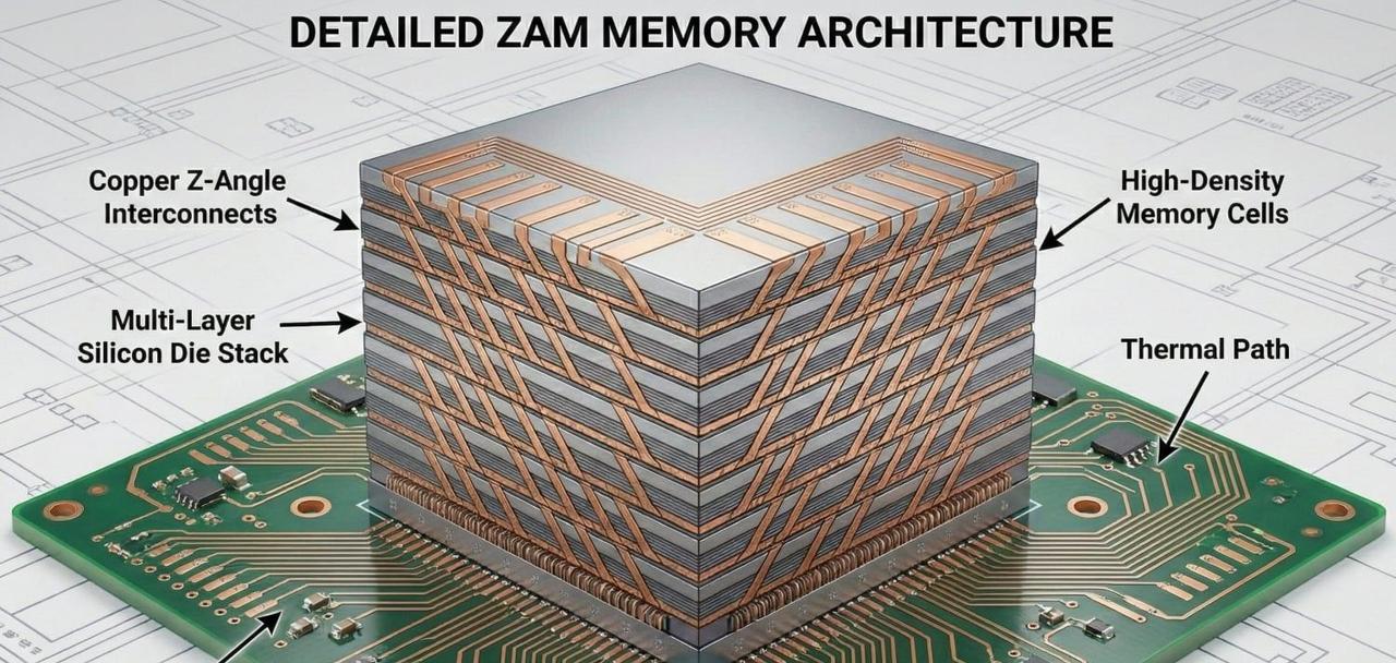
Intel is now looking to capitalize on the ongoing DRAM demand by partnering with a SoftBank subsidiary to launch a new "ZAM" memory technology. Well, with the AI infrastructure buildout being at its peak this year, there has been a gigantic rise in DRAM demand, driven by the adoption of hyperscalers and chip manufacturers. And more importantly, given that memory suppliers are limited worldwide, the supply chain bottleneck is immense right now, underscoring the need for new competitors to enter, which is why Intel is reported to be taking a new angle with the memory business. It is claimed that Team Blue will partner with SoftBank's Saimemory to develop a new standard called Z-Angle Memory (ZAM). It is reported that efforts to develop the ZAM memory technology had commenced under the Advanced Memory Technology (AMT) program initiated by the DoE, during which Intel showcased its "next-generation" DRAM bonding. Well, SoftBank's press release doesn't specifically discuss how the Z-Angle Memory is expected to be positioned. Still, based on what we know about Intel's DRAM bonding, ZAM would likely feature a staggered interconnect topology routing connections diagonally within the die stack rather than drilling straight down. Standard memory architectures cannot meet the needs of artificial intelligence. NGDB defines a completely new approach that will accelerate our move into the next decade. We are rethinking how DRAM is organized to fundamentally advance computer system architecture, aiming to achieve orders-of-magnitude performance improvements and incorporate innovation into industry standards. - Intel officials on next-gen DRAM bonding By the "Z-Angle" approach, Intel will effectively utilize a significant portion of the silicon area for memory cells, allowing higher densities and lower thermal resistance. Based on how the DRAM bonding technology could look, we could see ZAM using a copper-to-copper hybrid bonding, which enables more efficient inter-layer fusion and creates a "monolithic-like" silicon block rather than separate stacks. And since it is said that ZAM will be a capacitor-less design, we will see Intel's EMIB used to connect the memory to the AI chip. SoftBank's collaboration with Intel on ZAM ultimately allows it to own the memory stack as well, which we could see debut with the company's custom ASICs, such as the Izanagi lineup, giving the firm greater control over the architectural layout. While figures on the effective uplifts of ZAM versus HBM aren't specific for now, the Z-Angle approach provides the memory with better power efficiency and higher densities, ultimately enabling higher-layer stacking. Here's how HBM vs ZAM could play out: This isn't the first time Intel has pursued something in the DRAM segment; the company had a dedicated business around it, but it exited it in 1985 due to a drop in market share following competition from Japanese vendors. However, now that memory has created such a significant opportunity for companies, it would be interesting to see whether Intel's ZAM can make an impact, and one effective way to do so is by convincing leaders like NVIDIA to integrate the technology.
[8]
SoftBank Corp. Unit Teams Up With Intel to Work on Next-Generation Memory Tech -- Update
A unit of SoftBank. Corp is teaming up with Intel to develop cutting-edge memory technology that can better support artificial intelligence. The Japanese telecom company said Tuesday that subsidiary Saimemory will work on the technology with chip maker Intel, aiming to bring it to market in around 2029. According to people familiar with the matter, SoftBank plans to invest up to 3 billion yen, or about $19 million, over the next two years to advance the project, though the overall research-and-development cost has yet to be finalized. SoftBank said in a statement that the collaboration will focus on developing memory that can support high?capacity data processing and reduce power consumption in data centers used for training and running large-scale AI models. The pairing is strategic, coming as AI drives up memory costs and energy bills for data centers increasingly seen as key tech for national economic security. But analysts say it will take considerable time before a newcomer can pose any real challenge to the "Big Three" of memory makers: Samsung Electronics and SK Hynix of South Korea, and U.S. company Micron. For Intel and SoftBank to truly shake things up, they would likely need to partner with a current AI?chip leader like Nvidia, said Jukan Choe, an analyst with Citrini Research. The announcement comes as memory-chip companies grapple with a surge in demand from fast?growing AI firms that is squeezing already tight supplies. The market strain has intensified governments' efforts to secure more resilient chip supply chains, with countries like Japan and the U.S. stepping up cooperation on advanced manufacturing. Write to Yang Jie at [email protected] and Kosaku Narioka at [email protected]
Share
Share
Copy Link
Intel and SoftBank subsidiary Saimemory signed a collaborative agreement to develop Z-Angle Memory (ZAM), a vertically-stacked memory technology designed to compete with High Bandwidth Memory in AI data centers. The next-generation memory promises 2 to 3 times more capacity, greater bandwidth, and half the power consumption of HBM, with prototypes expected in 2027 and mass production targeted for 2029.
Intel Returns to Memory Business with Z-Angle Memory Development
Intel has signed a collaborative agreement with Saimemory, a SoftBank subsidiary, to advance the development of Z-Angle Memory (ZAM), marking the chipmaker's return to the memory market for the first time since the 1980s
1
. This next-generation memory technology is designed to compete directly with High Bandwidth Memory (HBM) used in AI data centers, but with significantly enhanced specifications. The vertically-stacked memory architecture promises to deliver 2 to 3 times the capacity of HBM while operating at half the power consumption and offering greater bandwidth1
. The partnership addresses a critical bottleneck in AI computing, as larger and more complex generative AI models demand advanced memory systems capable of handling massive data throughput while controlling energy costs5
.Source: Benzinga
Advanced DRAM Bonding Technology Powers ZAM Innovation
The Z-Angle Memory program builds on Intel's Next Generation DRAM Bonding (NGDB) initiative, which was completed under the Advanced Memory Technology R&D program managed by the U.S. Department of Energy and National Nuclear Security Administration through Sandia National Laboratory, Lawrence Livermore National Laboratory, and Los Alamos National Laboratory
3
. Saimemory will attempt to achieve these ambitious goals by vertically stacking more DRAM and using Intel's Embedded Multi-Die Interconnect Bridge (EMIB) to reduce latency between individual chips1
. The innovation builds on Intel's existing Foveros chip stacking technology, which first emerged in 2018 by extending Intel's EMIB technology vertically to allow stacking logic chips on top of one another3
. Dr. Joshua Fryman, Intel Fellow and CTO of Intel Government Technologies, explained that "Standard memory architectures aren't meeting AI needs, so NGDB defined a whole new approach to accelerate us through the next decade"1
.
Source: TweakTown
Production Timeline and Cost Advantages Target 2029 Commercialization
Saimemory is slated to produce its first ZAM prototypes sometime in 2027, with plans to develop a mass production line for the new memory by 2029
1
. According to reports from Nikkei, the DRAM bonding technology is designed to be up to 60% cheaper to produce than current HBM solutions1
. The partnership announced prototypes expected by the fiscal year ending March 31, 2028, with commercialization targeted for fiscal 20292
. Intel and Sandia had to design a new stacking approach and a different way of organizing the DRAM chips, with early prototypes confirming it was possible to increase capacity through new stacking techniques while recent developments have demonstrated the necessary high performance1
.
Source: PCWorld
Related Stories

Strategic Implications for AI Infrastructure and Japan's Semiconductor Revival
The collaboration extends the relationship between SoftBank Group and Intel, following SoftBank Group's mid-2025 agreement to invest $2 billion in the U.S. chipmaker
5
. This marks the first time a Japanese company has attempted to produce cutting-edge memory in decades, as Japan was a major memory manufacturing region in the 1980s before Korean and Taiwanese manufacturing dominated the market1
. Other firms backing the project include Japanese IT hardware and services firm Fujitsu, the recent Micron acquisition PowerChip Semiconductor Manufacturing, Shinko Electric Industries, and the University of Tokyo1
. Gwen Voskuilen, principal member of technical staff at Sandia, noted that "This is an exciting technology that we anticipate will lead to a wider adoption of higher bandwidth memories in systems that are currently unable to take advantage of high bandwidth memory due to its limited capacity and power constraints"1
. The venture positions memory density and power efficiency as critical factors for AI data centers processing large-scale AI models, while SoftBank views the development as a key initiative to support next-generation social infrastructure and strengthen Japan's global competitiveness in semiconductor technologies1
. Shares of SoftBank rose 3.13%, while Intel stock rose 5% in overnight trading following the announcement2
.References
Summarized by
Navi
[4]
[5]
Related Stories
Intel's Next-Gen AI Hardware: Jaguar Shores with HBM4 and Diamond Rapids with MRDIMMs
02 Jul 2025•Technology
D-Matrix Challenges HBM with 3DIMC: A New Memory Technology for AI Inference
04 Sept 2025•Technology
Nvidia Collaborates with Major Memory Makers on New SOCAMM Format for AI Servers
24 Mar 2025•Technology
Recent Highlights


Recent Highlights
Today's Top Stories


Your Daily Dose of Curated AI News
Don’t drown in AI news. We cut through the noise - filtering, ranking and summarizing the most important AI news, breakthroughs and research daily. Spend less time searching for the latest in AI and get straight to action.