Stanford team builds first commercial 3D chip at US foundry with 4x AI performance gains
2 Sources
2 Sources
[1]
First truly 3D chip fabbed at US foundry, features carbon nanotube transistors and RAM on a single die -- future devices could have up to 1000x improvement in energy-delay product
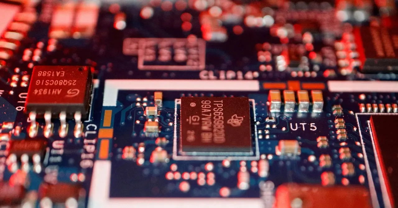
Prototype manufactured at SkyWater shows dense vertical memory-logic integration with measured and simulated AI speedups. A collaborative research team has demonstrated what it says is the first monolithic 3D integrated circuit manufactured at a commercial U.S. foundry, reporting substantial performance gains over conventional flat chip designs. The prototype was developed by engineers from Stanford, Carnegie Mellon, the University of Pennsylvania, and MIT, and fabricated in partnership with SkyWater Technology. The chip departs from conventional two-dimensional layouts by stacking memory and logic directly on top of one another in a single, continuous process. Instead of assembling multiple finished dies into a package, the researchers built each device layer sequentially on the same wafer using a low-temperature process designed not to damage underlying circuitry, resulting in a dense network of vertical interconnects that shortens data paths between memory cells and compute units. The prototype was manufactured on SkyWater's 200mm production line, using a mature 90nm to 130nm process. The stack integrates conventional silicon CMOS logic with resistive RAM layers and carbon nanotube field-effect transistors, all fabricated under a thermal budget of about 415°C. According to the team, early hardware tests show roughly a four-fold improvement in throughput compared with a comparable 2D implementation operating at similar latency and footprint. Beyond the measured hardware results, the researchers also evaluated taller stacks through simulation. Designs with additional tiers of memory and compute showed up to a twelve-fold performance improvement on AI-style workloads, including models derived from Meta's LLaMA architecture. The group further argues that the architecture could eventually deliver 100-fold to 1,000-fold improvements in energy-delay product, a combined metric of speed and efficiency, by continuing to scale vertical integration rather than shrinking transistors. While academic labs have previously demonstrated experimental 3D chips, the team emphasizes that this work differs in being built in a commercial foundry environment rather than a bespoke research line. SkyWater executives involved in the project described the effort as proof that monolithic 3D architectures can be transferred into domestic manufacturing flows, rather than remaining confined to university cleanrooms. "Turning a cutting-edge academic concept into something a commercial fab can build is an enormous challenge," said co-author Mark Nelson, vice president of technology development operations at SkyWater Technology. The team presented their research at the IEEE International Electron Devices Meeting (IEDM 2025) between December 6 and 10.
[2]
US engineers develop 3D chip that offers order-of-magnitude speed gains
Engineers in the United States have developed a novel multilayer computer chip with a unique architecture that could help usher in a new era of AI hardware and domestic semiconductor innovation. The team highlighted that in hardware tests and simulations, the new 3D chip outperforms 2D chips by roughly an order of magnitude. Unlike today's largely flat, 2D chips, the new prototype's key ultra-thin components rise like stories in a tall building, with vertical wiring acting like numerous high-speed elevators that enable fast, massive data movement. Its record-setting density of vertical connections and carefully interwoven mix of memory and computing units help the chip bypass the bottlenecks that have long slowed improvement in flat designs. "This opens the door to a new era of chip production and innovation," said Subhasish Mitra, the William E. Ayer Professor in Electrical Engineering and professor of computer science at Stanford University, and principal investigator of a new paper describing the chip presented at the 71st Annual IEEE International Electron Devices Meeting (IEDM). "Breakthroughs like this are how we get to the 1,000-fold hardware performance improvements future AI systems will demand." While academic labs have previously built experimental 3D chips, this is the first time such a chip has shown clear performance gains and been manufactured in a commercial foundry. The team also pointed out that on conventional 2D chips, components sit on a single, flat surface with limited, spread-out memory, so data must travel across a few long, crowded routes. Because the computing elements run much faster than the data can move - and because the chip can't store enough memory close by - the system ends up constantly waiting on information. Engineers call this bottleneck the "memory wall," the point at which processing speed outpaces the chip's ability to deliver data, according to a press release. "By integrating memory and computation vertically, we can move a lot more information much quicker, just as the elevator banks in a high-rise let many residents travel between floors at once," said Tathagata Srimani, assistant professor of electrical and computer engineering at Carnegie Mellon University, the paper's senior author, who began the work as a postdoctoral fellow advised by Mitra.
Share
Share
Copy Link
A Stanford-led research team has manufactured the first monolithic 3D integrated circuit at a commercial US foundry, showing four-fold performance improvements over conventional flat chips. The prototype, built at SkyWater Technology, vertically stacks memory and logic using carbon nanotube transistors and could eventually deliver up to 1,000-fold gains in energy efficiency for future AI systems.
First Commercial 3D Chip Manufactured at US Foundry
A collaborative research team from Stanford University, Carnegie Mellon University, MIT, and the University of Pennsylvania has fabricated what they claim is the first monolithic 3D integrated circuit at a commercial US foundry, marking a significant milestone for domestic semiconductor development. The prototype 3D chip was manufactured at SkyWater Technology's 200mm production line, demonstrating that advanced vertical chip architectures can transition from academic labs into real-world manufacturing environments
1
. While experimental 3D chips have been built before in university cleanrooms, this represents the first time such a design has been produced in a commercial foundry setting with measurable performance advantages.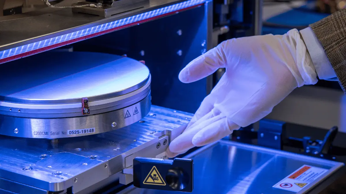
Source: Tom's Hardware
Vertical Architecture Delivers Order-of-Magnitude Speed Gains
The chip departs from conventional two-dimensional layouts by building a structure that vertically stacks memory and logic directly on top of one another in a single, continuous process. Instead of assembling multiple finished dies into a package, engineers built each device layer sequentially on the same wafer using a low-temperature process designed not to damage underlying circuitry
1
. This creates a dense network of vertical interconnects that dramatically shortens data paths between memory cells and compute units. Early hardware tests show roughly a four-fold improvement in throughput compared with a comparable 2D implementation operating at similar latency and footprint1
. The team highlighted that in both hardware tests and simulations, the new architecture delivers order-of-magnitude speed gains over traditional flat designs2
.Carbon Nanotube Transistors and Resistive RAM Integration
The prototype was manufactured using a mature 90nm to 130nm process that integrates multiple advanced technologies. The stack combines conventional silicon CMOS logic with resistive RAM layers and carbon nanotube field-effect transistors, all fabricated under a thermal budget of about 415°C
1
. This low-temperature approach is critical for building true 3D structures, as it prevents damage to underlying circuit layers during sequential fabrication. The record-setting density of vertical connections and carefully interwoven mix of memory and computing units help the chip overcome data bottlenecks that have long constrained flat chip designs2
.Breaking Through the Memory Wall for AI Hardware
The architecture directly addresses what engineers call the "memory wall," the point at which processing speed outpaces a chip's ability to deliver data. On conventional 2D chips, components sit on a single, flat surface with limited, spread-out memory, forcing data to travel across a few long, crowded routes
2
. "By integrating memory and computation vertically, we can move a lot more information much quicker, just as the elevator banks in a high-rise let many residents travel between floors at once," explained Tathagata Srimani, assistant professor at Carnegie Mellon University and senior author of the paper2
. This capability is particularly valuable for AI hardware, where massive data movement between memory and processors creates significant bottlenecks.Related Stories
Simulations Project 1000x Improvement in Energy-Delay Product
Beyond the measured hardware results, researchers evaluated taller stacks through simulation to understand future scaling potential. Designs with additional tiers of memory and compute showed up to a twelve-fold performance improvement on AI-style workloads, including models derived from Meta's LLaMA architecture
1
. The group argues that the architecture could eventually deliver 100-fold to 1,000-fold improvements in energy-delay product, a combined metric of speed and efficiency, by continuing to scale vertical integration rather than shrinking transistors1
. "This opens the door to a new era of chip production and semiconductor innovation," said Subhasish Mitra, principal investigator at Stanford University. "Breakthroughs like this are how we get to the 1,000-fold hardware performance improvements future AI systems will demand"2
.Commercial Viability and Domestic Manufacturing Implications
SkyWater executives involved in the project emphasized the significance of demonstrating that monolithic 3D architectures can be transferred into domestic manufacturing flows. "Turning a cutting-edge academic concept into something a commercial fab can build is an enormous challenge," said Mark Nelson, vice president of technology development operations at SkyWater Technology
1
. The team presented their research at the IEEE International Electron Devices Meeting (IEDM 2025) between December 6 and 101
. For the AI industry, this development suggests a potential path forward as traditional transistor scaling slows, offering a way to continue improving chip performance through vertical integration rather than relying solely on smaller feature sizes.References
Summarized by
Navi
[2]
Related Stories
MIT Engineers Develop 'High-Rise' 3D Chip Technology for Advanced AI Hardware
19 Dec 2024•Technology

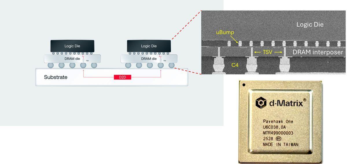
D-Matrix Challenges HBM with 3DIMC: A New Memory Technology for AI Inference
04 Sept 2025•Technology
NVIDIA Unveils Futuristic Vision for AI Compute: Silicon Photonics and 3D Stacking
11 Dec 2024•Technology

Recent Highlights
1
OpenAI Releases GPT-5.4, New AI Model Built for Agents and Professional Work
Technology

2
Anthropic sues Pentagon over supply chain risk label after refusing autonomous weapons use
Policy and Regulation

3
OpenAI secures $110 billion funding round as questions swirl around AI bubble and profitability
Business and Economy

Recent Highlights
Today's Top Stories


Your Daily Dose of Curated AI News
Don’t drown in AI news. We cut through the noise - filtering, ranking and summarizing the most important AI news, breakthroughs and research daily. Spend less time searching for the latest in AI and get straight to action.