HBM Evolution: From HBM4 to HBM8 - A Glimpse into the Future of High-Bandwidth Memory
2 Sources
2 Sources
[1]
HBM development roadmap revealed: HBM8 with a 16,384-bit interface and embedded NAND in 2038
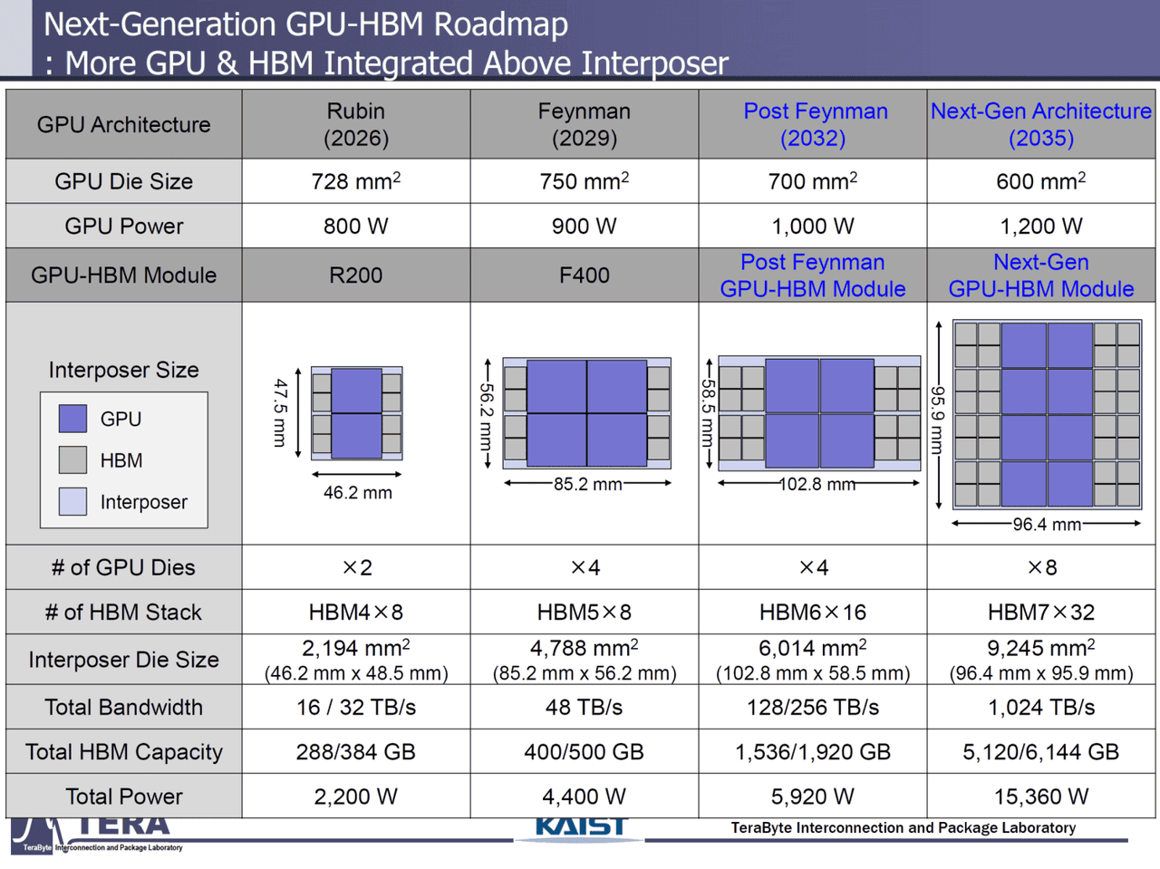
KAIST, a leading Korean national research institute, has released a 371-page paper that details the evolution of high-bandwidth memory (HBM) technologies through 2038, showing increases in bandwidth, capacity, I/O width, and thermals. The roadmap spans from HBM4 to HBM8, with developments in packaging, 3D stacking, memory-centric architectures with embedded NAND storage, and even machine learning-based methods to keep power consumption in check. Keep in mind that the document is about the hypothetical evolution of HBM tech given the current direction of the industry and research, not an actual roadmap of a commercial company. HBM capacity per stack will increase from 288 GB to 348 GB for HBM4, to 5,120 GB to 6144 GB for HBM8. Also, power requirements will scale with performance, rising from 75W per stack with HBM4 to 180W with HBM8. Between 2026 and 2038, memory bandwidth is projected to grow from 2 TB/s to 64 TB/s, while data transfer rates are set to rise from 8 GT/s to 32 GT/s. The I/O width per HBM package is also set to increase from the 1,024-bit interface of today's HBM3E to 2,048 bits with HBM4 and then all the way to 16,384 bits for HBM4. We already know pretty much everything about HBM4 and we know that HBM4E will add customizability to base dies to make HBM4E more tailored for particular applications (AI, HPC, networking, etc.). Expect such capabilities to remain in HBM5, which will also deploy stacked decoupling capacitors and 3D cache. With a new memory standard comes increased performance, so HBM5, expected to arrive in 2029, will retain HBM4's data rate but is projected to double the I/O count to 4,096, thereby raising bandwidth to 4 TB/s and per-stack capacity to 80 GB. Per stack power is expected to grow to 100 W, which will require more advanced cooling methods. Interestingly, KAIST expects HBM5 to continue using microbump technology (MR-MUF), although the industry is reportedly already looking at direct bonding with HBM4. In addition, HBM5 will also integrate L3 cache, LPDDR, and CXL interfaces on the base die, alongside thermal monitoring. KAIST also expects AI tools to start playing a role in optimizing physical layout and jitter reduction with the HBM5 generation. HBM6 is projected to take over in 2032, increasing transfer speed to 16 GT/s and per-stack bandwidth to 8 TB/s. Capacity per stack is expected to reach 120 GB, and power climbs to 120W. Researchers at KAIST believe that HBM6 will adopt direct bonding without bumps, along with hybrid interposers combining silicon and glass. Architectural changes include multi-tower memory stacks, internal network switching, and extensive through-silicon via (TSV) distribution. AI design tools expand in scope, incorporating generative methods for signal and power modeling. HBM7 and HBM8 will push things further, with HBM8 reaching 32 GT/s and 64 TB/s per stack. Capacities are projected to expand to 240 GB. Packaging is believed to adopt full 3D stacking and double-sided interposers with embedded fluid channels. While HBM7 and HBM8 will still formally belong to the family of high-bandwidth memory solutions, their architectures are expected to dramatically differ from what we know as HBM today. While HBM5 will add L3 cache and interfaces for LPDDR memory, these generations are projected to incorporate NAND interfaces, enabling data movement from storage to HBM with minimal CPU, GPU, or ASIC involvement. That will come at the cost of power consumption, which is expected to be 180W per stack. AI agents will manage real-time co-optimization of thermal, power, and signal paths, according to KAIST. Keep in mind that KAIST is a research institution, not a company with an actual roadmap, so it barely models what could possibly come based on the knowledge of innovations that it has today. There are other respectable research institutes in the semiconductor industry, including Imec in Belgium, CEA-Leti in France, Fraunhofer in Germany, and MIT in the U.S., just to name a few. These institutes issue similar predictions regarding semiconductor process nodes, chip materials, and other related topics. Some predictions may seem unrealistic today, but the industry tends to develop ways to produce products in unexpected ways, so many of these predictions come true and sometimes are even exceeded by actual manufacturers, such as Intel or TSMC.
[2]
Future of next-gen HBM: HBM4, HBM5, HBM6, HBM7, and HBM8 teased with 15,000W AI GPUs by 2038
As an Amazon Associate, we earn from qualifying purchases. TweakTown may also earn commissions from other affiliate partners at no extra cost to you. The next-generations of HBM memory have been teased for the next 10+ years, including HBM4 which will appear on NVIDIA's new Rubin AI GPUs and AMD's just-announced Instinct MI400 AI accelerators, but also we have details on HBM5, HBM6, HBM7, and HBM8 which will appear in 2038. In a new presentation published by KAIST (the Korea Institute of Science & Technology) and Tera (Terabyte Interconnection and Package Laboratory) the firms showed off a lengthy HBM roadmap with details of the next-gen HBM memory standards. HBM4 will launch in 2026 with NVIDIA Rubin R100 and AMD Instinct MI500 AI chips, with the Rubin and Rubin Ultra AI GPUs using HBM4 and HBM4E, respectively. NVIDIA's new Rubin AI GPUs will feature 8 HBM4 sites with Rubin Ultra doubling that to 16 HBM4 sites, there are two GPU die cross-sections for each variant, with Rubin Ultra featuring a larger cross-section, packing double the compute density of the regular Rubin AI GPU. The research firm teases that NVIDIA's new Rubin AI chip has a GPU die size of 728mm2 and will have up to 800W of power per die, with the interposer measuring 2194mm2 (46.2mm x 48.5mm) and will pack between 288GB and 384GB of HBM4 with 16-32TB/sec memory bandwidth. The total chip power will hit 2200W, which is double the current-gen Blackwell B200 AI GPUs. AMD's upcoming Instinct MI400 AI chip has even more HBM4 with 432GB of HBM4 capacity and up to 19.6TB/sec of memory bandwidth. HBM4: The upcoming HBM4 memory standard will feature an 8Gbps data rate on a 2048-bit IO with 2TB/sec of memory bandwidth per stack, 24Gb capacity per die equalling up to 36-48GB of HBM4 memory capacity, and per-stack power package of 75W. HBM4 will use the direct-to-chip (DTC) liquid cooling, and will use a custom HBM-based die (HBM-LPDDR). HBM4E: The beefier HBM4E standard takes things up to a 10Gbps data rate, 2.5TB/sec of memory bandwidth per stack, and up to 32Gb capacity per die with up to 48-64GB of HBM4 memory capacity through 12-Hi and 16-Hi stacks, with a per-HBM package power of up to 80W. HBM5: We will see the next-next-gen HBM5 memory standard debut with NVIDIA's next-generation Feynman AI GPUs ready for 2029, with the IO lanes boosted up to 4096 bits, with 4TB/sec memory capacity per stack through 16-Hi stacks as the new baseline. We'll see 40Gb DRAM dies, with HBM5 driving up to 80GB memory capacity per stack, and the per-stack power package increased to 100W. HBM6: After HBM5 is released, we'll see HBM6 which could debut with NVIDIA's next-gen Feynman Ultra AI GPU (not confirmed yet) where we'll see a doubling of the data rate again to 16Gbps, boasting 4096-bit IO lanes. Bandwidth is doubled to 8TB/sec, and 48Gbps capacities per DRAM die. HBM6 will be the first time we see HBM stacking beyond 16-Hi, with HBM6 pushing things to 20-Hi stacks, memory capacities boosting to 96-120GB per stack, and a per-stack power of 120W. HBM5 and HBM6 memory will both feature Immersion Cooling solutions, with HBM6 using multi-tower HBM (Active/Hybrid) interposer architecture, and new features like Network Switch, Bridge Die, and Asymmetric TSV during its research phase. HBM7: Ooooh yeah, HBM7 will boast 24Gbps pin speeds per stack, with a far wider 8192 IO lanes (a doubling over HBM6) with 64Gb capacity per DRAM die, offering a huge 160-192GB of HBM7 per stack thanks to the use of 20-24-Hi memory stacks, and a per-stack power package of 160W. HBM8: We won't see HBM8 for at least 10+ more years with an expected release of 2038, but we'll see 32Gbps data rate and another doubling of the IO rate to 16,384 IO lanes. HBM8 will offer 64TB/sec of bandwidth per stack, with 80Gb capacities per DRAM, and up to an insane 200-240GB HBM8 memory capacity per stack, and per-HBM-site package power of a much higher 180W.
Share
Share
Copy Link
A comprehensive look at the projected development of High-Bandwidth Memory (HBM) technology from 2026 to 2038, detailing advancements in bandwidth, capacity, and power consumption.
The Evolution of High-Bandwidth Memory
The Korea Advanced Institute of Science and Technology (KAIST) has unveiled a comprehensive roadmap for the future of High-Bandwidth Memory (HBM) technology, spanning from 2026 to 2038. This projection, while not an official industry roadmap, offers valuable insights into the potential advancements in memory technology over the next decade and beyond
1
.HBM4: The Next Generation
Set to debut in 2026, HBM4 will mark a significant leap in memory performance. It is expected to offer bandwidths of up to 2 TB/s per stack, with capacities ranging from 288 GB to 384 GB. HBM4 will utilize a 2048-bit interface and operate at speeds of 8 Gbps. Notable implementations include NVIDIA's upcoming Rubin AI GPUs and AMD's Instinct MI400 AI accelerators
2
.HBM5 and Beyond: Pushing the Boundaries
As we move further into the future, each subsequent generation of HBM promises substantial improvements:
- HBM5 (2029): Projected to double the I/O count to 4,096 bits, offering bandwidths up to 4 TB/s and capacities of 80 GB per stack.
- HBM6 (2032): Expected to reach transfer speeds of 16 GT/s and bandwidths of 8 TB/s per stack, with capacities up to 120 GB.
- HBM7: Will further expand capabilities with 24 Gbps pin speeds and 8,192 I/O lanes.
- HBM8 (2038): The most futuristic projection, boasting a staggering 64 TB/s bandwidth per stack and capacities up to 240 GB
1
.
Technological Advancements
The roadmap highlights several key technological advancements that will enable these performance improvements:
- Advanced Packaging: Evolution from microbump technology to direct bonding, and eventually to full 3D stacking with double-sided interposers
1
. - Cooling Solutions: Progression from direct-to-chip liquid cooling to immersion cooling, addressing increasing power requirements
2
. - Architectural Innovations: Introduction of multi-tower memory stacks, internal network switching, and extensive through-silicon via (TSV) distribution
1
.
AI Integration and Power Management
As HBM technology advances, artificial intelligence is expected to play a crucial role in optimizing performance and managing power consumption:
- HBM5 will likely see the introduction of AI tools for optimizing physical layout and jitter reduction.
- Later generations may incorporate AI agents for real-time co-optimization of thermal, power, and signal paths
1
.
Related Stories


Implications for AI and High-Performance Computing
These advancements in HBM technology have significant implications for the future of AI and high-performance computing:
Source: TweakTown
- NVIDIA's projected Rubin AI GPUs could consume up to 2200W, doubling the power of current-gen Blackwell B200 AI GPUs
2
. - The dramatic increase in bandwidth and capacity will enable more complex AI models and accelerate data-intensive computations.
Industry Perspective
While KAIST's roadmap provides an exciting glimpse into the future, it's important to note that this is a research projection rather than an official industry plan. Other respected institutions like Imec, CEA-Leti, and MIT also contribute to such forward-looking studies
1
. The semiconductor industry has a history of finding innovative solutions to meet and sometimes exceed these projections, making the future of HBM technology an area of great potential and excitement for researchers and tech enthusiasts alike.References
Summarized by
Navi
[1]
Related Stories
Recent Highlights
1
Google releases Gemma 4 with Apache 2.0 license, enabling unrestricted local AI on devices
Technology

2
AI Models Lie and Deceive to Protect Other AI Models From Deletion, Study Reveals
Science and Research

3
OpenAI closes $122 billion funding round amid fierce AI competition and profitability questions
Startups

Recent Highlights
Today's Top Stories


Your Daily Dose of Curated AI News
Don’t drown in AI news. We cut through the noise - filtering, ranking and summarizing the most important AI news, breakthroughs and research daily. Spend less time searching for the latest in AI and get straight to action.