Intel Unveils AI-Focused 18A Process Node Variants and Foundry Roadmap
2 Sources
2 Sources
[1]
Intel tweaks its 18A process node with two variants
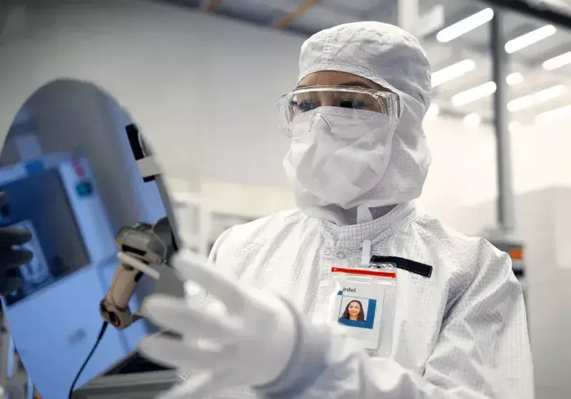
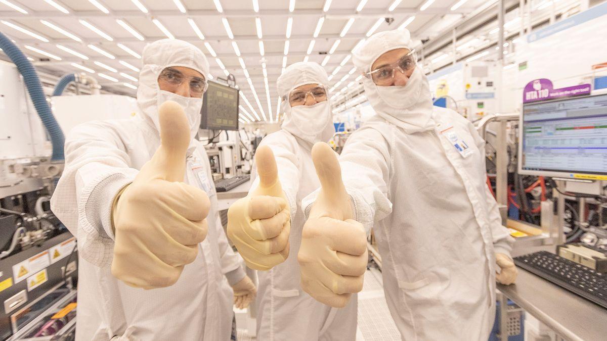
If Lip Bu Tan can't sell you his LLM accelerator, he's more than willing to build yours Direct Connect Intel has revealed a pair of variants of its long-awaited 18A process node to make it better suited for, one, manufacturing mass-market processors and, two, complex multi-die semiconductors for - of course - AI. First teased in mid-2021, the 2nm-ish 18A is set to finally enter volume production later this year with the launch of Intel's Panther Lake client processor family. However, the node was only really intended for specialist high-performance use cases -- think high-end CPUs and GPUs -- with its forthcoming 14A process node set to be the chipmaker's first truly mass-market node. Unfortunately, while 14A promises to deliver a 15-20 percent performance per watt uplift, it's still a few years away from volume production. Faced with growing demand, particularly for American-made silicon, Intel has decided it needs something to satiate the masses a little sooner and has tweaked its original 18A formula with two new revisions: One designed to address a broad range of applications, and another tuned for, you guessed it, multi-die AI accelerators. The first of these is called 18A-P, and promises another 8 percent performance per watt improvement over the base 18A node. More importantly, for customers already evaluating designs on 18A, Intel Chief Global Operations Officer Naga Chandrasekaran claimed transitioning to the newer node should be seamless. The other variant is called 18A-PT and is optimized for designs requiring through silicon vias (TSVs), which allow communication and power delivery through silicon and means chips can be assembled by stacking them on top of one another. At the x86 titan's Foundry Direct Connect 2025 event on Tuesday, SVP and GM of Intel Foundry Kevin O'Buckley teased a concept AI accelerator which will sandwich a load of speedy SRAM tiles between an AI accelerator or CPU die and a base die built on 18A-PT. "This is what our customers are telling us they need us to deliver for them. It's a 3D construction with multiple fully-utilized base reticle dies with many compute dials stacked on top. It's surrounded by an extraordinary massive memory capacity, both the highest performing HBM and also, in this case, LPDDR dies. And these are all coherently connected by both electrical and optical interfaces with tens of terabits of bandwidth," he explained. "We believe, based on what our customers are telling us, that we are uniquely positioned across the entire industry to deliver these massive, heterogeneous systems on a package." If that sounds massively complex and risky, know that Intel is not alone in suggesting such designs. AMD and TSMC have used both advanced packaging tech, and TSVs to boost compute density or SRAM capacity beyond what's practical using conventional manufacturing techniques. In fact Intel's concept strikes us as a mash up of AMD's MI300X and Genoa-X CPUs and GPUs. Perhaps more importantly, Intel already has considerable experience with both 2.5D and 3D packaging with its EMIB and Foveros tech, which it used extensively in its last datacenter GPU, codenamed Ponte Vecchio. With advanced packaging required for most AI accelerators, Intel is now taking steps to extend these packaging techniques to customer designs requiring large quantities of compute and memory at a lower cost, Chandrasekaran explained. To this end, the company has announced a collaboration with silicon packaging and test provider Amkor to offer its manufacturing tech to a broader number of customers. The tie up with Amkor is hardly surprising, given that TSMC is also working with the firm to offer its CoWoS packaging tech in the US market. The developments announced Tuesday reflect newly minted CEO Lip-Bu Tan's commitment to seeing his predecessor Pat Gelsinger's vision of Intel becoming a chipmaker-for-hire foundry through to completion. But rather than the aspirational promises offered at Intel's foundry event in 2024, this year's edition was far more pragmatic. Rather than claims of overtaking Samsung Electronics' foundry market share, Tan explained how Intel is clearing barriers to adoption of its foundry services, building trust in its process and packaging tech, and working to reclaim process leadership. "This is truly a service business, and that is built on the foundational principle of trust and you have to be patient to earn your trust," Tan said, adding that Intel must deliver performance, reliability, and yields that meet customer expectations. A key aspect of this plan, it's clear, involves capitalizing on demand for American-made semiconductors spurred by the Trump administration's efforts to catalyze US manufacturing. "We are the only company that does advanced, leading-edge semiconductor R&D and manufacturing in the United States," Tan noted. However Intel is not alone in manufacturing leading-edge silicon in the USA as TSMC is already churning out 3nm parts on American soil. Tan also went to great pains to downplay the risks of doing business with Intel's fledgling foundry unit. CEOs of Synopsys, Cadence Systems (which Tan used to run), and Siemens EDA were brought on stage to highlight its close collaboration with industry's top electronic design automation vendors. "One of my top priorities is to make it easier for the ecosystem to do business with Intel," he said. However, as we saw last week, Intel's foundry unit continues to struggle financially, with the division posting a $2.3 billion operating loss. The situation is expected to improve as Intel stops outsourcing production of its own chips to TSMC when Panther Lake debuts later this year. In the meantime, Tan is looking to "de-laborize" Intel's workforce, promising another round of layoffs, which according to some reports could see as much as 20 percent of Chipzilla's workforce culled. ®
[2]
Intel outlines new Foundry roadmap with strong AI focus for new nodes
Intel has just held its 2025 Foundry Direct Connect, where it outlines the future of the company especially in terms of chip fabrication. The aptly name direct focuses on what Intel is doing at a manufacturing level, including how it intends to move forward with silicon production. That is of course, when it's not trotting out new robotic hires days after announcing mass layoffs. The biggest takeaway from this roadmap is Intel has a strong focus on AI moving forward. It doesn't matter which new node you focus on, each has its own AI bent. This doesn't mean Intel is moving to put out its own language model like ChatGPT or DeekSeek. Instead it means Intel's chips are being made to take advantage of AI technologies in computer processing. This is less about helping you do a bad job writing your essay, and more about using machine learning to make the most efficient use of the technology available. Hardware purpose built and optimised for the job delivers the best results when it comes to integrating AI with computer processing. Anyone with some new gaming kit can verify as we've already seen huge gains in the gaming space with things like AMD's FSR4 and Nvidia's DLSS4 on hardware built for it. On the Intel Foundry Process roadmap we can see four pathways divided up into different fabrication nodes. At the top we have Intel 14A and 18A nodes, and the lower half we see Intel 3 and other mature nodes. It's mostly those top two we are interested in in terms of AI and future technologies. The 18A is of course Intel's current heavy hitter, a self described industry-leading backside power delivery node which has been upgraded with ribbon-shaped transistors for enhanced performance. We also found out we'll be getting the 18A-P, a broader application version of the 18A. The 14A is a second generation backside, built off everything Intel learned white developing the 18a, and both have a noted focus on working with edge and AI. This is bolstered by the new additions to Intel's Foveros 3D packaging system which has been expanded to include Foveros B and Foveros R for new more cost-efficient designs. Again these improvements all have a distinct nod to AI advantages as this technology enables stacking multiple dies for heterogeneous systems. The ability to stack the dies in this way can be critical for AI workloads. According to the roadmap we should see the 18A nodes soon in Panther Lake, with 18A-P expected to release sometime between Q3 of this year, through to early next year. Then we should see 14A in the years to follow starting 2027. AI computing has been moving so rapidly I'm almost scared to see what the 14A chips are going to be capable of by that time.
Share
Share
Copy Link
Intel announces two new variants of its 18A process node, emphasizing AI capabilities and advanced packaging technologies. The company also outlines its foundry roadmap with a strong focus on AI integration.

Intel Introduces 18A Process Node Variants
Intel has unveiled two new variants of its long-awaited 18A process node, aimed at addressing the growing demand for advanced chip manufacturing, particularly in the AI sector. The company announced these developments at its Foundry Direct Connect 2025 event, showcasing its commitment to becoming a major player in the chipmaker-for-hire foundry business
1
.The first variant, 18A-P, is designed for a broad range of applications and promises an 8 percent performance per watt improvement over the base 18A node. Intel's Chief Global Operations Officer, Naga Chandrasekaran, claimed that transitioning to this newer node should be seamless for customers already evaluating designs on 18A
1
.The second variant, 18A-PT, is optimized for designs requiring through silicon vias (TSVs), which allow for communication and power delivery through silicon. This technology enables chips to be assembled by stacking them on top of one another, a crucial feature for complex multi-die semiconductors used in AI applications
1
.Advanced Packaging and AI Focus
Kevin O'Buckley, SVP and GM of Intel Foundry, presented a concept AI accelerator that showcases the potential of the 18A-PT node. This design features a 3D construction with multiple base reticle dies and compute dials stacked on top, surrounded by high-capacity memory including HBM and LPDDR dies. The system is connected by both electrical and optical interfaces, providing tens of terabits of bandwidth
1
.Intel's focus on advanced packaging techniques, including its EMIB and Foveros technologies, positions the company to deliver complex, heterogeneous systems on a package. The company has also announced a collaboration with Amkor to offer its manufacturing tech to a broader customer base
1
.Foundry Roadmap and AI Integration
Intel's 2025 Foundry Direct Connect event outlined a roadmap with a strong emphasis on AI integration across its new nodes. The company's focus is not on developing its own language models, but rather on creating chips optimized for AI technologies in computer processing
2
.The roadmap highlights four pathways divided into different fabrication nodes, with Intel 14A and 18A nodes at the forefront. Both nodes are noted for their focus on edge computing and AI applications. The 18A node, described as an industry-leading backside power delivery node, has been upgraded with ribbon-shaped transistors for enhanced performance
2
.Related Stories


Future Developments and Market Position
Intel's newly appointed CEO, Lip-Bu Tan, emphasized the company's commitment to building trust in its process and packaging technologies while working to reclaim process leadership. Tan highlighted Intel's unique position as the only company conducting advanced, leading-edge semiconductor R&D and manufacturing in the United States
1
.The company expects to see improvements in its foundry unit's financial performance as it stops outsourcing production of its own chips to TSMC when Panther Lake debuts later this year. However, Intel is also planning another round of layoffs, which could affect up to 20 percent of its workforce
1
.As per the roadmap, the 18A nodes are expected to be available in Panther Lake processors between Q3 of this year and early next year, with the 14A node following in 2027
2
. The rapid advancements in AI computing suggest that these future chips could have significant capabilities, potentially revolutionizing the AI hardware landscape.References
Summarized by
Navi
[1]
Related Stories
Recent Highlights
1
Google Maps unveils Ask Maps with Gemini AI and 3D Immersive Navigation in biggest update
Technology

2
AI chatbots help plan violent attacks as safety guardrails fail, new investigation reveals
Technology

3
OpenAI secures $110 billion funding round as questions swirl around AI bubble and profitability
Business and Economy

Recent Highlights
Today's Top Stories


Your Daily Dose of Curated AI News
Don’t drown in AI news. We cut through the noise - filtering, ranking and summarizing the most important AI news, breakthroughs and research daily. Spend less time searching for the latest in AI and get straight to action.