Scintil Photonics begins shipping laser chips to customers, targets AI data center demand
4 Sources
4 Sources
[1]
AI Data Centers Get a Laser Boost With Optical Networking
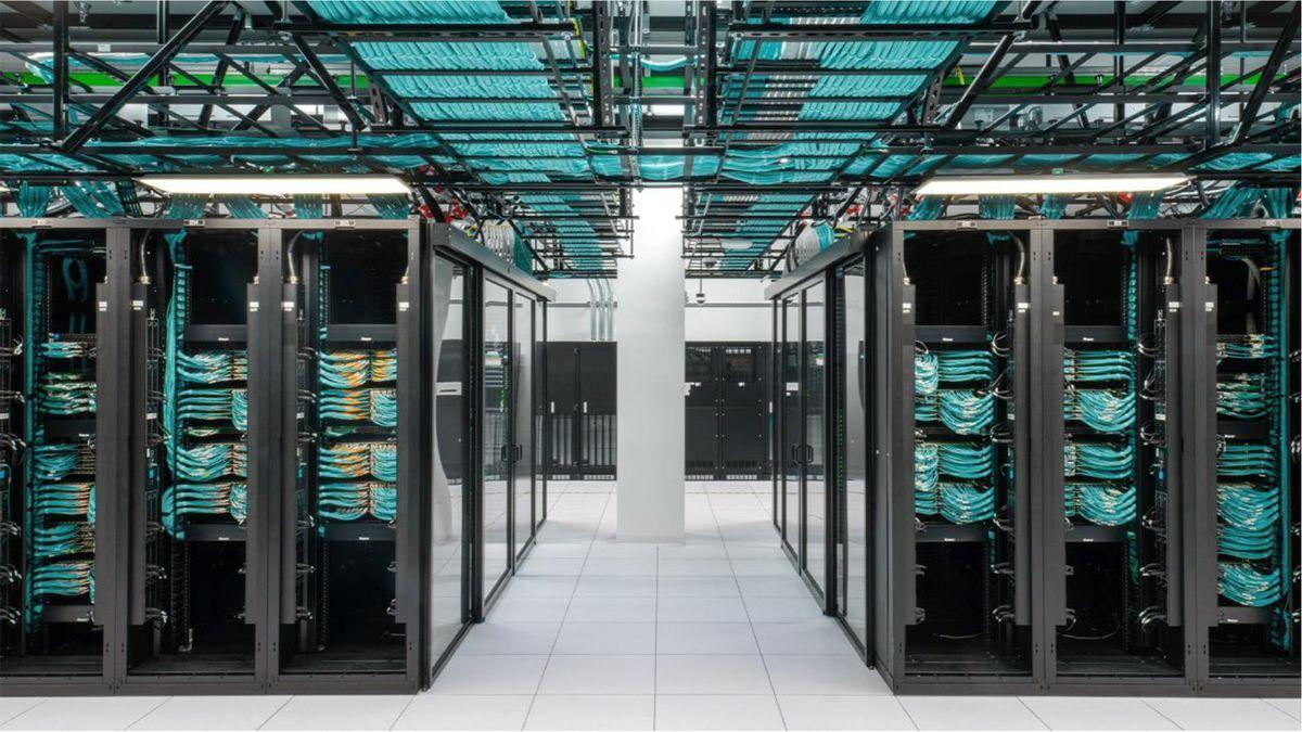
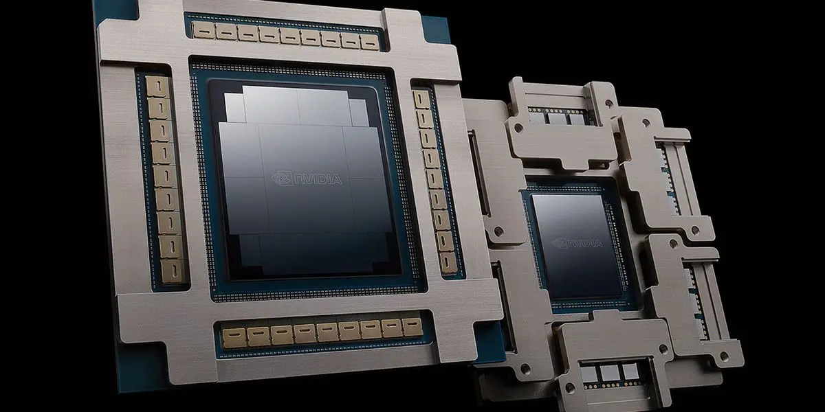
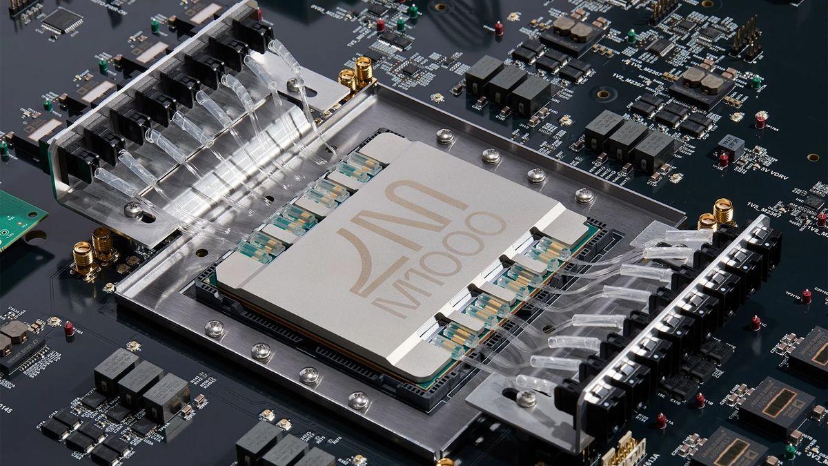
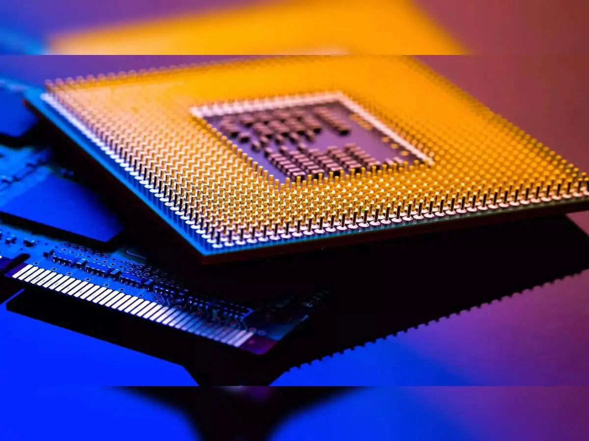
As the bandwidth and power demands of AI data centers necessitate a transition from electrical to optical scaleup networking, one component has been conspicuously absent from the co-packaged optics arsenal: the laser itself. That's no longer the case. Last month, Tower Semiconductor and Scintil Photonics announced production of the world's first single-chip DWDM light engine for AI infrastructure. DWDM, or dense wavelength division multiplexing, transmits multiple optical signals over a single fiber -- greatly reducing power and latency while connecting dozens of GPUs. Matt Crowley, the CEO of Scintil Photonics, says that the idea of multiplexing optically is not new. Indeed, it's been around as long as the internet itself. In the 1990s, telecom companies buried huge amounts of optical fiber in the streets, assuming that one wavelength per fiber would eventually become the norm. When the telecom industry realized it possible to transport tens of wavelengths down a single fiber via multiplexing, it revolutionized the industry. The reason that DWDM has not yet been deployed for data centers specializing in AI applications is that the technology is not yet scalable for cost and needs. "The data transmitted within an AI data center is the equivalent of massively scaling a supercomputer," Crowley says. In particular, the challenge arises in scale-up networking, or directly connecting accelerators (XPUs, or extended processing units) within a rack or cluster -- as opposed to scale-out networking, which connects separate clusters within a data center. Optimizing dozens of GPUs and memory to function as a single entity demands seamless bandwidth and extremely low latency. To increase bandwidth, reduce latency, and improve energy efficiency in AI data centers, network engineers have gradually been replacing copper links with optical ones. Pluggable transceivers convert electrical signals to optical and vice versa, via discrete optical components integrated onto a single chip: co-packaged optics, or CPO. "Everything that a big chip company makes involves bonding an optical chip onto their GPU," says Crowley. The CPO becomes an input/output chip for the processor. But without a scalable way to integrate lasers themselves into the same silicon process flow, it's been impossible to feed multiple wavelengths per fiber onto one chip. Scintil and Tower will discuss their manufacturing roadmap and details at at the OFC 2026 Conference 17 to 19 March in Los Angeles. Scintil's "SHIP" (Scintil Heterogeneous Integrated Photonics) technology integrates lasers, photodiodes, modulators, and other components onto a mass-produced silicon wafer. "It's our version of CMOS," says Crowley, but with a few tricks to get around the intrinsic challenges of binding an optical gain material to silicon. The process starts with a standard 300-millimeter silicon photonics wafer, complete with passive optical components, from Tower Semiconductors. Next, the wafer is flipped upside down to expose its buried oxide layer. Bonding tiny squares of un-patterned InP/III-V semiconductor dies to that layer, precisely where they're needed at each laser site, minimizes the amount needed of the expensive semiconductor material. Finally, photolithography tools etch diffraction gratings to form eight distributed feedback lasers. "We're not re-inventing the laser," says Crowley. Rather, the advanced photolithography tools translate into more precise spacing and wavelength stability than traditional manufacturing could provide on a silicon wafer. The final product is the "LEAF Light" photonic integrated circuit, a chip that integrates two sets of eight distributed feedback arrays. Each fiber port delivers eight or 16 wavelengths with 100 or 200 gigahertz channel spacing, to ensure no overlap or mode hopping. A second ASIC chip hosts all the electronics to control and monitor the laser array. "This is building the laser onto the CPO chip," says Crowley. Nvidia and Broadcomm have already deployed CPO with a single wavelength per fiber, proving its workability in scale-out networking. "We're enabling next-generation CPO for scale-up." Transmitting multiple wavelengths through a single fiber moves the industry toward a desirable "slow and wide" architecture. For example, instead of transmitting 400 Gb/s over a single channel, or wavelength, the LEAF Light chip spreads 50 Gb/s over 8 channels, greatly increasing the data capacity per fiber and overall power efficiency. The design enables up to 1.6 terabit per second data speeds in a single fiber, and a recent Nvidia roadmap suggested that future DWDM interconnects could eventually enable sub-1 picojoule per bit operations. Perhaps the most important benefit, according to Crowley, is in latency. "I need to maintain low latency between GPUs," he says. If any individual processor operates faster than the network overall, the GPUs are always waiting for data bits to process -- a problem that's amplified in scale-up networks with tens or hundreds of GPUs. Forward-processing and error-correction on high-bandwidth channels increases the odds of poor latency. "The utilization rate of the GPUs just tanks," says Crowley. Using low-bandwidth DWDM to connect multiple GPUs can double utilization. Scintil and Tower will provide tens of thousands of units to customers by the end of 2026, and plan to increase production by an order of magnitude next year. By 2028, when customers intend to deploy DWDM in scale-up networks, the supply chain will be ready for them. "We're excited about the possibilities it could open up," says Crowley.
[2]
Nvidia-backed startup Scintil Photonics starts testing laser chips with customers
SAN FRANCISCO, March 11 (Reuters) - Scintil Photonics, a French startup backed by Nvidia, on Wednesday said it has started providing laser chips to customers for testing. Scintil is one of a number of startups working out how to move information around inside artificial intelligence servers such as those made by Nvidia (NVDA.O), opens new tab and Advanced Micro Devices (AMD.O), opens new tab using pulses of light rather than electrical signals, a move that could ease the task of linking many chips together to form one large computer. Analysts expect Nvidia to reveal more about its plans for the technology, called co-packaged optics, at its developer conference in Silicon Valley next week. All optical systems rely on a laser chip to generate the beams of light that will carry information, and those chips, made with a special material called indium phosphide and mostly used in long-distance communications networks, are not currently made in large enough volumes to meet the demand from AI data centers. That supply dynamic drove Nvidia earlier this month to invest $2 billion each in two of the largest makers of those lasers, Lumentum (LITE.O), opens new tab and Coherent (COHR.N), opens new tab. Scintil, which secured funding from Nvidia in a $58 million funding round last year, has come up with a way to package indium phosphide lasers with some of the other elements needed for optical communications into a single chip, working with Israel-based Tower Semiconductor (TSEM.TA), opens new tab as a manufacturing partner. Matt Crowley, Scintil's CEO, said the company is in discussions with "six companies, seven companies" that want to use its technology by 2028 but declined to name them, citing nondisclosure agreements. He said Scintil's goal is to be able to produce hundreds of thousands of chips per month by then. "The way we make it is fundamentally different," Crowley said in an interview. "We can mass produce them ... and we can satisfy a big chunk of the market." Reporting by Stephen Nellis in San Francisco; Editing by Chizu Nomiyama Our Standards: The Thomson Reuters Trust Principles., opens new tab
[3]
Nvidia-backed Scintil Photonics begins shipping AI laser chips
Scintil Photonics, a French startup backed by Nvidia, has begun providing laser chips to customers for testing. The company is developing optical technology to move data using light instead of electrical signals, aiming to ease linking many chips together in AI servers. Analysts expect Nvidia to reveal more about its co-packaged optics plans at its developer conference in Silicon Valley next week. The development addresses a critical supply constraint in the AI hardware market. Laser chips made with indium phosphide are currently not produced in large enough volumes to meet data center demand. Nvidia invested $2 billion each in laser makers Lumentum and Coherent earlier this month to address this shortage. Scintil secured funding from Nvidia in a $58 million funding round last year. The company partnered with Israel-based Tower Semiconductor to package indium phosphide lasers with other optical communication elements into a single chip. This integration aims to simplify the manufacturing process for AI server components. Scintil's CEO Matt Crowley said the company is in discussions with six to seven companies that want to use its technology by 2028. Crowley stated that Scintil aims to produce hundreds of thousands of chips per month by that year. He declined to name the potential customers, citing nondisclosure agreements. Crowley said the company's manufacturing method is fundamentally different from existing approaches. He stated that Scintil can mass produce the chips and satisfy a big chunk of the market demand.
[4]
Nvidia-backed startup Scintil Photonics starts testing laser chips with customers
Scintil Photonics, a French startup backed by Nvidia, on Wednesday said it has started providing laser chips to customers for testing. Scintil is one of a number of startups working out how to move information around inside artificial intelligence servers such as those made by Nvidia and Advanced Micro Devices using pulses of light rather than electrical signals, a move that could ease the task of linking many chips together to form one large computer. Analysts expect Nvidia to reveal more about its plans for the technology, called co-packaged optics, at its developer conference in Silicon Valley next week. All optical systems rely on a laser chip to generate the beams of light that will carry information, and those chips, made with a special material called indium phosphide and mostly used in long-distance communications networks, are not currently made in large enough volumes to meet the demand from AI data centers. That supply dynamic drove Nvidia earlier this month to invest $2 billion each in two of the largest makers of those lasers, Lumentum and Coherent. Scintil, which secured funding from Nvidia in a $58 million funding round last year, has come up with a way to package indium phosphide lasers with some of the other elements needed for optical communications into a single chip, working with Israel-based Tower Semiconductor as a manufacturing partner. Matt Crowley, Scintil's CEO, said the company is in discussions with "six companies, seven companies" that want to use its technology by 2028 but declined to name them, citing nondisclosure agreements. He said Scintil's goal is to be able to produce hundreds of thousands of chips per month by then. "The way we make it is fundamentally different," Crowley said in an interview. "We can mass produce them ... and we can satisfy a big chunk of the market."
Share
Share
Copy Link
Nvidia-backed Scintil Photonics has started providing laser chips to customers for testing, marking a breakthrough in optical networking for AI data centers. The French startup partnered with Tower Semiconductor to produce single-chip DWDM light engines that transmit data using light instead of electrical signals. With plans to produce hundreds of thousands of chips monthly by 2028, the company aims to address critical supply constraints in the AI hardware market.
Scintil Photonics Delivers Breakthrough Laser Chips for Optical Networking
Scintil Photonics has begun shipping laser chips to customers for testing, addressing one of the most critical bottlenecks in AI data centers
2
. The French startup, backed by Nvidia through a $58 million funding round last year, partnered with Tower Semiconductor to produce the world's first single-chip DWDM light engine specifically designed for AI infrastructure1
. This technology enables networks to transmit data using light rather than electrical signals, a transition essential for linking multiple AI chips together to function as one large computer2
.
Source: IEEE
Matt Crowley, CEO of Scintil Photonics, revealed that the company is in discussions with six to seven companies interested in deploying this technology by 2028, though he declined to name them due to nondisclosure agreements
4
. The company aims to produce hundreds of thousands of chips per month by that timeframe, positioning itself to satisfy a significant portion of market demand3
.Addressing Supply Constraints in the AI Hardware Market
The development comes at a crucial moment for the AI hardware market. Indium phosphide lasers, essential components for optical systems that generate beams of light to carry information, are not currently manufactured in large enough volumes to meet demand from AI data centers
2
. This supply dynamic prompted Nvidia to invest $2 billion each in Lumentum and Coherent, two of the largest makers of these lasers, earlier this month3
.Scintil's approach fundamentally differs from traditional manufacturing methods. The company has developed a way to package indium phosphide lasers with other elements needed for optical communications into a single photonic integrated circuit
4
. "The way we make it is fundamentally different," Crowley stated. "We can mass produce them ... and we can satisfy a big chunk of the market"2
.DWDM Technology Enables Scale-Up Networking for GPUs
The technology relies on dense wavelength division multiplexing, or DWDM, which transmits multiple optical signals over a single fiber, greatly reducing power consumption and latency while connecting dozens of GPUs
1
. While DWDM has been used in telecommunications since the 1990s, it hasn't been deployed for AI data centers due to scalability challenges related to cost and specific needs1
.The challenge lies particularly in scale-up networking—directly connecting accelerators within a rack or cluster rather than connecting separate clusters. Optimizing dozens of GPUs and memory to function as a single entity demands seamless bandwidth and extremely low latency
1
. Co-packaged optics, which integrate discrete optical components onto a single chip, have been gradually replacing copper links to increase bandwidth, reduce latency, and improve power efficiency1
.Related Stories
Manufacturing Innovation Through Silicon Photonics Integration
Scintil's "SHIP" (Scintil Heterogeneous Integrated Photonics) technology integrates lasers, photodiodes, modulators, and other components onto a mass-produced silicon wafer
1
. The process begins with a standard 300-millimeter silicon photonics wafer from Tower Semiconductor, complete with passive optical components. The wafer is then flipped to expose its buried oxide layer, where tiny squares of un-patterned InP/III-V semiconductor dies are bonded precisely at each laser site, minimizing the amount of expensive semiconductor material needed1
.
Source: ET
The final product, called the "LEAF Light" photonic integrated circuit, integrates two sets of eight distributed feedback arrays. Each fiber port delivers eight or 16 wavelengths with 100 or 200 gigahertz channel spacing to prevent overlap or mode hopping
1
. This design enables up to 1.6 terabit per second data speeds in a single fiber, with data capacity spread across multiple channels for improved power efficiency1
. A recent Nvidia roadmap suggested that future DWDM interconnects could eventually enable sub-1 picojoule per bit operations1
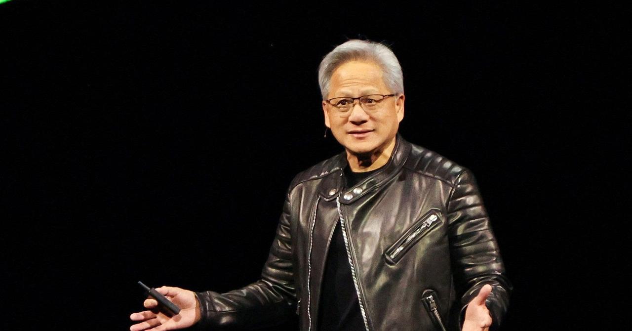
.Analysts expect Nvidia to reveal more details about its plans for co-packaged optics at its developer conference in Silicon Valley, highlighting the growing importance of optical networking solutions in the AI infrastructure landscape
2
.References
Summarized by
Navi
Related Stories
Recent Highlights


Recent Highlights
Today's Top Stories


Your Daily Dose of Curated AI News
Don’t drown in AI news. We cut through the noise - filtering, ranking and summarizing the most important AI news, breakthroughs and research daily. Spend less time searching for the latest in AI and get straight to action.