Nvidia Set to Pioneer TSMC's Advanced A16 Node, Reshaping AI Chip Landscape
4 Sources
4 Sources
[1]
Nvidia tipped to be TSMC's first 16A customer, ahead of Apple -- Feynman GPUs could make full use of GAA transistors and backside power
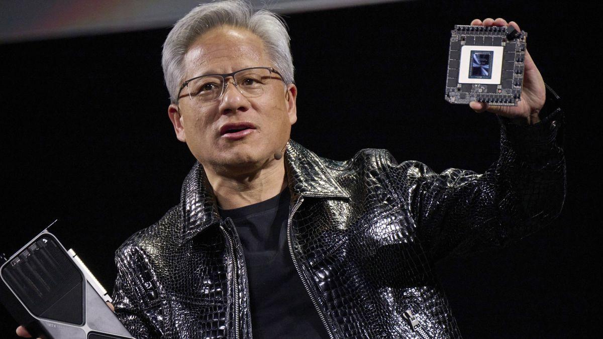
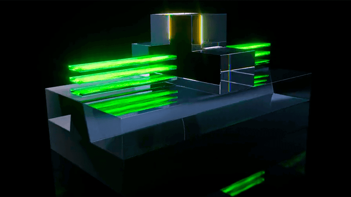
For the first time, an AI GPU will launch on TSMC's bleeding edge. Nvidia will be the first customer to use TSMC's A16 node, a 1.6nm-class process that marries gate-all-around (GAA) transistors with backside power delivery, according to China's Commercial Times. This is no small change in tradition: For more than a decade, Apple has been the one to break in each new process node from TSMC, with its iPhone SoCs serving as the high-volume anchor tenant. But that tradition ends here. A16's first customer isn't building phones; its chips are designed for AI and other applications with extreme power delivery requirements. As TSMC's first commercial node to integrate backside power delivery -- which lifts power rails off the front and routes them through the back of the wafer -- the foundry is pitching A16 as the natural progression from its N2 process. If reports that Nvidia plans to skip this N2 process for its upcoming Feynman architecture in favor of A16 are true, that could make Feynman the first GPU, and the first chip of any kind, to combine GAA and backside power in production. Nvidia has historically waited for process maturity before adopting new nodes. Hopper was on TSMC's 4N, not N5, and Blackwell's data center products use 4NP. Feynman potentially changes that by putting Nvidia at the bleeding edge, ahead of even Apple, suggesting that the company views AI as the driver of its most advanced silicon. A16 is more than a shrink. It's the first TSMC process to feature both GAA nanosheet transistors and backside power delivery. By shifting power delivery to the backside, signal routing on the front side becomes less constrained, reducing congestion and improving performance. Power reaches the transistors via a shorter, less resistive path, thereby reducing voltage drop and enabling higher frequencies or tighter integration. TSMC claims that A16 delivers 8-10% higher speed or 15-20% lower power compared to baseline N2, plus a modest 7-10% density gain. The real benefit isn't in the numbers, but rather what they unlock. With more available routing and cleaner power, large chips like GPUs gain new architectural freedom with wider cores, larger caches, more AI engines, and better scaling. And because backside power delivery frees front-side metal for signals, it simplifies high-density hybrid bonding on the top surface. This makes 3D-stacked cache or vertically integrated SRAM more practical, and eases front-side congestion around wide I/O like HBM physical layers (PHYs), provided the design also employs fine-pitch hybrid bonding and adequate thermal mitigation at the package level. Nvidia's decision to lead with A16 suggests that GPU designs are now pressing against front-side power delivery limits on advanced nodes. Moving power to the backside shortens the supply path and frees front-side interconnect, mitigating IR drop and routing congestion that become bottlenecks. In other words, these factors are turning backside power delivery into an architectural necessity for AI and HPC applications. It also helps Nvidia leapfrog the competition. AMD is reportedly targeting standard 2nm for its next-gen EPYC and MI400-class accelerators. Intel's 18A node is also expected to offer backside power through PowerVia around the same time. By moving straight to A16, Nvidia avoids this middle ground entirely and could potentially land with a full node advantage over its rivals with a chip based on Feynman architecture as early as 2028. Naturally, gaining this edge won't be cheap. Wafer pricing for A16 is rumored to exceed $30,000 based on N2 pricing, which far exceeds Apple's typical wafer costs. But for Nvidia, where a single AI GPU can retail for tens of thousands, that premium might be easier to absorb. More importantly, Nvidia is betting that the node's density and efficiency gains will more than offset the cost and lock in the company's lead for the second half of the decade. Handing A16's debut to Nvidia is a calculated shift for Nvidia. While Apple remains a major partner and is still expected to adopt baseline N2 for its 2026 iPhone 18 chips, Nvidia's AI chips offer faster demand growth and a use case that showcases the A16's strengths. AI chips are power hungry, bandwidth-constrained behemoths sensitive to layout limitations -- and A16 has been built to address all these things. It's also not unthinkable to see this as a hedge against Intel. With its 18A process approaching, which also features a backside power solution, TSMC needs a flagship customer to prove it can execute at the same or higher level. Getting Feynman out the door on A16 before Intel gets any third-party 18A designs will help to reinforce TSMC's leadership. If Feynman on A16 is a success, it will ultimately set the tone for the next generation of AI silicon. Nvidia will have proven that backside power is not just viable but essential for extreme compute. That could force AMD, Intel, and others to accelerate their own roadmap decisions or risk falling behind on performance. It may also reshape how packaging and architectures evolve. Designers will need new thermal models and power domain strategies to work with backside power delivery. Still, Nvidia's status as the first to move in this territory will give it a leg-up in tooling and methodology -- advantages that are difficult to copy.
[2]
Nvidia is rumoured to be first in line to use TSMC's ultra-advanced A16 chip node, although it's AI GPUs that'll likely see the benefit first
Somewhat surprisingly, Nvidia doesn't have much of a track record when it comes to using cutting-edge silicon. But a new report claims that's about to change dramatically, with Nvidia planning to be the very first to use TSMC's next-next gen A16 node. Taiwanese outlet CTEE claims that Nvidia will be the first to adopt TSMC's A16 node due to competition from AMD, in part for what it calls HPC or high performance chips built on TSMC's upcoming N2 node and due out this year. The only N2 chips AMD has planned for next year, as far as we know, are server CPUs, not GPUs. AMD's next major AI GPU release, MI450, is expected to be on TSMC N3 silicon. Nvidia currently uses a version of TSMC's N4 node for all its GPUs. N4 is actually a refinement of N5, which dates back to 2020. Meanwhile, the first chip made on TSMC's N3 technology, the Apple A17 Pro SoC for iPhones, debuted back in 2023. Consequently, Nvidia is now bumping up against what's known as the reticle limit with its Blackwell generation of GPUs. That's a physical limit on the size of an individual chip that can be etched onto a wafer. That physical size in turn puts a hard limit on how many transistors can be squeezed into a single chip. Nvidia's most powerful AI GPU, GB200, actually uses a pair of reticle-sized GPUs fused together on a single interposer. Nvidia's RTX 5090 GPU, codenamed GB202, is likewise up pretty close to TSMC's N4 reticle limit at 750mm2. Indeed, Nvidia essentially carried over N4 production technology from the previous RTX 4090 family to the current RTX 50 GPUs. That's one important reason why the likes of the RTX 5070 and RTX 5080 are barely any better than their direct progenitors. For Nvidia's next-gen Rubin generation, Nvidia will be using TSMC's N3 node. But if this news about TSMC A16 is correct, Nvidia could skip N2 altogether and jump straight to A16. Of course, the immediate question with all of this is how relevant it is to gaming. The idea that Nvidia might want to accelerate it's AI roadmap onto A16 makes a lot of sense. But gaming GPUs? The thing is, Nvidia's approach for multiple generations now has been to used a shared GPU architecture across both AI and gaming and produce all chips on the same node. Obviously an AI GPU is very different to a gaming GPU. But certain elements of the chips, such as at least parts of the Tensor cores, are like the same on all chips. That makes it cheaper and faster to engineer GPUn designs for a given node. Thus, Nvidia's current Blackwell GPUs are all on N4 and its next-gen Rubin GPUs, including both AI and gaming variants, are expected to be on N3. This TSMC A16-related report, if accurate, would apply to the generation after Rubin, which is known as Feynman and is due out in 2028. If it turns out that Nvidia is indeed skipping N2 and that includes gaming GPUs, too, then it could be very good news. Nvidia will have many more transistors to play with in a couple of generations' time as a consequence. And you'd normally expect that to translate into significantly higher performance and perhaps new features. Of course, Nvidia also has form for launching disappointingly incremental GPU upgrades, such as Blackwell. But as I said, part of the problem with Blackwell is the old TSMC node. So, this A16 rumour for the Feynman generation could be very positive news for PC gaming. As ever, we'll ultimately have to wait and see.
[3]
NVIDIA rumored to be the first customer for TSMC's most advanced A16 process node in 2026
TL;DR: NVIDIA is poised to be the first customer for TSMC's advanced A16 process node in late 2026, responding to AMD's lead with TSMC's 2nm AI chips. This move highlights the industry's shift toward cutting-edge semiconductor technology, emphasizing enhanced performance and chip density despite high production costs. NVIDIA could very well be the first customer for TSMC's most advanced, next-generation A16 process node in 2026, as it "feels heat from AMD" which is using TSMC's newest nodes for its dominant CPUs coming to market. In a new report from Taiwanese media outlet Ctee picked up by @DanNystedt on X, we're hearing that NVIDIA could be the first customer for TSMC's next-gen A16 process node in 2H 2026. Most of the new 2nm chips coming off the production lines at TSMC will be for smartphones -- mostly Apple and MediaTek -- but AMD will have the first 2nm AI chip, which has prompted NVIDIA to consider the A16 node with backside power delivery (BSPD). If NVIDIA does indeed use TSMC's new A16 node, it would be the first time that an AI chip was first to use the very latest TSMC process technology, knocking off smartphones from that claim. Semiconductor industry analysts have said that although 2nm is expensive -- citing Apple's new 2nm chip wafers for the next-gen iPhone 18 costing close to $27,000 each, and NVIDIA's backside power supply version costing over $30,000 -- that this is a significant increase both in performance and chip density, making it the "key reason' for many customers to "pay for value".
[4]
NVIDIA Reportedly Set to Be TSMC's First A16 (1.6nm) Customer, Likely Being Influenced By AMD's Push For High-End AI GPUs
NVIDIA is claimed to be TSMC's first A16 node customer, and this move marks a unique shift in the firm's approach, since it had tended to rely on older processes from the Taiwan giant. Well, it seems that NVIDIA plans to improve the performance of its future AI architectures, and the firm will depend on TSMC to achieve this goal. Traditionally, NVIDIA wasn't one of the first customers to use cutting-edge nodes from the Taiwan giant, and instead, firms like Apple, MediaTek, and Qualcomm relied on TSMC's most recent nodes. But, based on a report by Ctee, it is claimed that there's going to be a massive shift in approach from Team Green, as it will be the first to utilize the A16 process, which is set to feature huge performance uplifts, and of course, comply with Moore's Law fundamentals. It is claimed that since 110nm, NVIDIA hasn't been the first to rely on TSMC's cutting-edge nodes, and instead, the firm has focused on architectural advancements to scale up performance. It seems like the A16 process will pan out to be a 'momentual' release by TSMC, mainly driven by how the Taiwan giant will introduce technologies such as Gate-All-Around FETs (GAAFET) and Super Power Rail (SPR) backside power delivery. The more important factor here is SFR over all other advancements, but we'll talk about this sometime later. NVIDIA's pivot towards the A16 node could come in late 2027 or early 2028, considering that TSMC plans HVM by late 2026. Based on the firm's roadmap, we could see the technology's debut either with Rubin Ultra or Feynman GPUs, but the latter lineup is a higher possibility, considering that Feynman will feature several other advancements as well. For TSMC, this is indeed great news, since every mainstream AI hardware manufacturer will employ the company's high-end nodes, which will ultimately contribute to the revenue from the process generation.
Share
Share
Copy Link
Nvidia is rumored to be the first customer for TSMC's cutting-edge A16 process node, marking a significant shift in the semiconductor industry. This move could give Nvidia a competitive edge in AI chip development and alter the dynamics of high-performance computing.
Nvidia's Strategic Shift to TSMC's A16 Node
In a surprising turn of events, Nvidia is rumored to be the first customer for TSMC's cutting-edge A16 process node, marking a significant shift in the semiconductor industry
1
2
. This move breaks the long-standing tradition of Apple being the first to adopt TSMC's latest nodes for its iPhone SoCs1
.
Source: Wccftech
A16 Node: A Technological Leap
The A16 node, a 1.6nm-class process, represents a significant advancement in semiconductor technology. It combines two critical innovations:
- Gate-all-around (GAA) transistors
- Backside power delivery
This combination offers substantial improvements over previous nodes, with TSMC claiming 8-10% higher speed or 15-20% lower power compared to the baseline N2 process
1
.Implications for Nvidia's AI Dominance
Nvidia's decision to lead with A16 suggests that GPU designs are now pressing against front-side power delivery limits on advanced nodes
1
. By adopting A16, Nvidia could potentially:- Gain a full node advantage over rivals
- Unlock new architectural freedoms for wider cores, larger caches, and more AI engines
- Simplify high-density hybrid bonding, making 3D-stacked cache or vertically integrated SRAM more practical
1
Source: PC Gamer
Competitive Landscape and Industry Impact
This move is seen as a response to competition from AMD, which is reportedly targeting standard 2nm for its next-gen EPYC and MI400-class accelerators
3
. By skipping the N2 process and moving straight to A16, Nvidia could potentially leapfrog the competition1
2
.
Source: TweakTown
Related Stories
Timeline and Future Prospects
The A16 node is expected to be ready for high-volume manufacturing by late 2026
4
. Nvidia's adoption of this technology could come in late 2027 or early 2028, potentially with the Feynman GPU architecture4
.While the cost of A16 wafers is rumored to exceed $30,000, industry analysts believe the significant increase in performance and chip density justifies the investment for high-value applications like AI chips
3
.Potential Impact on Consumer GPUs
While the immediate focus is on AI chips, Nvidia's historical approach of using a shared GPU architecture across both AI and gaming suggests that consumer GPUs could also benefit from this advanced node in the future
2
. This could translate into significantly higher performance and new features for gaming GPUs in the coming years.References
Summarized by
Navi
[1]
[3]
Related Stories
AMD's 2nm Leap: Challenging Nvidia's AI GPU Dominance with Next-Gen Instinct MI450
09 Oct 2025•Technology

TSMC's 3nm Process Set for Massive Adoption by AI Tech Giants
15 Oct 2024•Technology

NVIDIA CEO Jensen Huang Predicts 20% Performance Boost from GAA Technology, Emphasizes Architectural Innovations
27 Mar 2025•Technology
Recent Highlights
1
Tennessee Teens Sue Elon Musk's xAI Over Grok AI-Generated Child Abuse Images
Policy and Regulation

2
Pentagon designates Palantir Maven AI as core US military system in major defense shift
Technology

3
Supermicro Co-Founder Indicted in $2.5 Billion Nvidia AI Chip Smuggling Scheme to China
Policy and Regulation
Recent Highlights
Today's Top Stories


Your Daily Dose of Curated AI News
Don’t drown in AI news. We cut through the noise - filtering, ranking and summarizing the most important AI news, breakthroughs and research daily. Spend less time searching for the latest in AI and get straight to action.