Samsung's HBM3E Memory Breakthrough: Nvidia Certification Boosts AI Chip Competition
6 Sources
6 Sources
[1]
Samsung earns Nvidia certification for its HBM3 memory -- stock jumps 5% as company finally catches up to SK hynix and Micron in HBM3E production
Investor confidence reflects Samsung's efforts to regain its technology lead. Samsung's 12-layer HBM3E chips have passed Nvidia's qualification tests for use in high-end AI accelerators. The Korean giant's stock price immediately jumped over 5% following the news, as the certification means Samsung is catching up to SK hynix and Micron, both of which were already selling HBM3E chips to Nvidia. The welcome development comes around 18 months after HBM3E's development was complete, and after multiple certification delays. Samsung reportedly won't be selling HBM3E to Nvidia in high quantities until 2026, as current orders for the speedy chips are being fulfilled by SK hynix and Micron. According to the report, Samsung's HBM3 memory is expected to go into Nvidia DGX B300 cards in fairly short order, as Bloomberg's industry sources expect the chips will get the final Nvidia certification quite soon. As for AMD, Samsung was already selling HBM3E chips for Instinct MI350 cards, alongside Micron. HBM3 is currently the top grade of memory chips available, comprising 12 layers, up from eight in standard HBM3. This configuration results in a meaty 1.2 TB/s per stack. While HBM3E isn't even one year old, the AI train waits for no man. All sights are already set on HBM4, a spec that doubles the chips' bus width, resulting in approximately 2 TB/s of bandwidth per stack. It's worth noting that while the JEDEC HBM4 spec asks for 8 Gbps per pin, all three major memory makers are aiming for 10 to 11 GBps per pin on production chips, reportedly due to pressure from Nvidia. Thanks to manufacturing on 3-4 nm processes (down from 10 nm), HBM4 is predicted to offer significantly higher capacity of 64 GB per chip (up from 48 GB), along with a 20 to 30% reduction in power consumption. Samsung has been in talks with almost every AI chip maker to get an early certification for its upcoming HBM4 wares, intending to fire up volume production as soon as the first half of 2026. This particular race is currently led by SK hynix, which signaled the completion of its HBM4 development not even two weeks ago. Judging by Samsung's stock price jump, though, it seems investors are quite confident that the Korean maker will catch up soon enough.
[2]
Samsung overcomes technical challenges, ready to supply HBM3E chips to Nvidia
Serving tech enthusiasts for over 25 years. TechSpot means tech analysis and advice you can trust. Highly anticipated: Samsung Electronics is the world's largest memory manufacturer and one of the few companies with full chipmaking capabilities through its foundry facilities. But until recently, the Korean giant had fallen short of supplying the high-bandwidth memory Nvidia requires for its most powerful AI servers. That has now changed. Samsung Electronics has resolved the technical hurdles it faced in producing 12-layer HBM3E memory chips, successfully passing Nvidia's strict qualification tests. According to people familiar with the matter cited by KED Global, the Korean chipmaker will soon begin supplying the high-bandwidth memory required for Nvidia's AI servers. Sources said Samsung completed development of its HBM3E product about 18 months ago but initially failed to meet Nvidia's performance standards. Earlier this year, Jun Young-hyun, head of Samsung's semiconductor division, ordered a redesign of the DRAM core, a change that reportedly resolved the thermal issues seen in earlier versions. With those problems addressed, Samsung is now cleared to provide HBM3E chips to Nvidia, though volumes will remain limited for the time being. The company becomes the third supplier of such memory to the GPU maker, joining rivals SK hynix and Micron, and is expected to play only a secondary role in the near term. Samsung's ability to meet Nvidia's strict power and performance requirements is less about revenue and more about prestige, according to insiders. The achievement signals that the Korean manufacturer is back on track with its technology advancements. HBM3E chips are highly sought-after components, and AMD is already using Samsung-made memory in its MI350 accelerators. Nvidia is expected to deploy the memory in additional B300 servers, designed to significantly accelerate AI inference and training workloads. The HBM3E technology was first introduced by SK hynix in 2023 and is currently used by Nvidia in data center accelerators based on the Blackwell GPU microarchitecture. Meanwhile, the memory industry is shifting its focus to HBM4, the next-generation high-bandwidth memory standardized by JEDEC in April 2025. All major memory manufacturers are racing to bring HBM4 products to market, with SK hynix preparing mass production for Nvidia and other major customers. Industry insiders say Samsung's early performance indicators for HBM4 are promising, and the company plans to deliver its first HBM4 samples to Nvidia for validation later this month.
[3]
Samsung finally passes NVIDIA's strict HBM3E 12-Hi qualification tests: 10,000 units on the way
TL;DR: Samsung Electronics has passed NVIDIA's strict HBM3E 12-Hi memory qualification, securing a contract to supply 10,000 units for NVIDIA's AI GPUs. This marks a significant shift as Samsung challenges SK hynix's exclusive supply, positioning itself strongly for the upcoming HBM4 memory standard in next-gen AI hardware. Samsung Electronics has finally passed NVIDIA's strict HBM3E 12-Hi memory qualification tests for use on its AI GPUs, with the South Korean memory giant ready to supply 10,000 units. In a new report from AlphaEconomy picked up by insider @Jukanrosleve on X, NVIDIA recently signed a supply contract for its HBM3E 12-Hi memory to NVIDIA, where the contract will see Samsung supply around 10,000 units of its qualified HBM3 12-Hi product. Samsung commented, saying that everything is "progressing as scheduled". In previous rumors, Samsung's new HBM3E 12-Hi memory supply was confirmed, but this seems more solid and now a contract is in place, after fellow South Korean memory rival SK hynix has been exclusively supplying NVIDIA with all of the high-end HBM3 and HBM3E memory it needed. NVIDIA will use the next-gen HBM4 memory standard on its next-gen Rubin AI GPUs and AI servers, with Samsung performing what it hopes to be a huge turnaround in its semiconductor business. We reported just last week that NVIDIA initially requested 9Gbps speeds from HBM4, but pushing for upwards of 11Gbps. Samsung was the only one to offer HBM4 that could hit 10Gbps+ speeds, with SK hynix needing to pump more voltage (power + heat) to hit those 10Gbps speeds, and US-based Micron said 10Gbps was impossible... so Samsung is looking in great shape for the HBM4 fight in 2026.
[4]
Nvidia Greenlights Samsung's AI Chip Technology, Sets Stage For HBM4 Battle: Report - Intel (NASDAQ:INTC), Micron Technology (NASDAQ:MU)
Samsung Electronics Co. SSNLF has reportedly received the green light from Nvidia Corp. NVDA for its latest high-bandwidth memory (HBM3E) product, marking a significant breakthrough in the AI hardware chip supply race. Samsung Wins Nvidia Nod For HBM3E Memory Chips Samsung's fifth-generation 12-layer HBM3E product has passed Nvidia's qualification tests, according to sources familiar with the matter, reported KED Global on Friday. This approval comes after a year and a half of development and several unsuccessful attempts to meet Nvidia's stringent performance standards. Check out the current price of NVDA stock here. The approval is a significant milestone for Samsung, symbolizing a recovery of its technological credibility in a fiercely contested sector of the semiconductor industry. The HBM3E chips are slated to be used in Nvidia's flagship B300 AI accelerator and the MI350 from Advanced Micro Devices Inc. (AMD). Samsung Shares climbed nearly 5% in the Korean stock market on Monday. Supply To Stay Limited Despite Approval The approval from Nvidia is a significant win for Samsung, as it signifies a return to form in the competitive semiconductor industry. This development is particularly noteworthy in light of the increasing importance of AI hardware, which is driving the demand for high-capacity memory chips. Although Samsung has received approval, its supply of HBM3E chips to Nvidia is expected to remain limited, since it is the third company to gain clearance after SK Hynix Inc. and Micron Technology Inc. MU. The competition is moving to HBM4, set to launch with Nvidia's next-gen Vera Rubin chips next year, with Nvidia pushing suppliers to raise speeds beyond 10 Gbps from the current 8 Gbps standard. See Also: Netflix Co-Founder Reed Hastings Says Trump's $100,000 H-1B Visa Fee Is A 'Great Solution' Because Of These Reasons Nvidia Expands Its Partnership Base Nvidia's validation of Samsung's HBM3E chips comes at a time when the company is expanding its customer base and partnerships, especially in the wake of its recent chip ban in China. A semiconductor partnership between Nvidia and Intel Corp INTC could benefit both companies, but Nvidia is seen as the clear winner in the tie-up. This validation could further strengthen Nvidia's position in the market. Benzinga's Edge Rankings place Nvidia in the 93rd percentile for quality and the 98th percentile for growth, reflecting its strong performance in both areas. Check the detailed report here. READ NEXT: Intel Stock Has Best Day Ever: Jensen Huang Says Nvidia Will Be A 'Very Large Customer' Image via Shutterstock Disclaimer: This content was partially produced with the help of AI tools and was reviewed and published by Benzinga editors. INTCIntel Corp$29.48-3.57%OverviewMUMicron Technology Inc$162.25-3.93%NVDANVIDIA Corp$176.00-0.14%SSNLFSamsung Electronics Co Ltd$42.480.34%Market News and Data brought to you by Benzinga APIs
[5]
Samsung Shares Surge 5% After Clearing NVIDIA's HBM3E Performance Tests
Samsung Clears NVIDIA Tests for AI Memory Chips, Boosting Supply Prospects and Stock Performance Samsung Electronics has advanced in the global semiconductor market after reports confirmed its 12-layer HBM3E memory chips . The qualification marks a crucial step for Samsung as it works to expand its role in supplying high-bandwidth memory used in artificial intelligence accelerators. According to industry sources, NVIDIA is expected to finalise certification of soon. The approval comes at a time of strong demand for AI hardware, with HBM playing a central role in powering advanced models such as ChatGPT and DeepSeek. The development lifted Samsung's stock nearly 5% in South Korea on Monday, sending the shares to a one-year high. US-listed shares also recorded gains, while competitors such as Micron posted declines due to growing competitive pressure.
[6]
Samsung passes Nvidia's qualification test for 12-layer HBM3E chip - report By Investing.com
Investing.com -- Samsung Electronics has successfully passed Nvidia's qualification test for its 12-layer HBM3E product, according to a report from Korea Economic Daily that cited people familiar with the matter. The approval comes approximately 18 months after Samsung completed the development of the chip, the newspaper reported. The qualification represents a significant milestone for Samsung in the high-bandwidth memory market, potentially positioning the company to supply these advanced memory chips to Nvidia for use in its graphics processing units and artificial intelligence accelerators. This article was generated with the support of AI and reviewed by an editor. For more information see our T&C.
Share
Share
Copy Link
Samsung Electronics has successfully passed Nvidia's strict qualification tests for its 12-layer HBM3E memory chips, marking a significant comeback in the AI hardware race. This development has boosted investor confidence and set the stage for future competition in HBM4 technology.
Samsung's HBM3E Breakthrough
Samsung Electronics has achieved a significant milestone in the AI hardware race by successfully passing Nvidia's strict qualification tests for its 12-layer HBM3E (High Bandwidth Memory) chips
1
2
. This development comes after 18 months of efforts and multiple certification delays, marking a significant comeback for the Korean tech giant in the competitive semiconductor industry1
.
Source: TweakTown
Market Impact and Competition
The news of Samsung's certification led to an immediate 5% jump in the company's stock price, reflecting increased investor confidence
1
5
. Samsung is now poised to challenge the dominance of SK hynix and Micron, who were previously the exclusive suppliers of HBM3E chips to Nvidia3
.
Source: Analytics Insight
Supply and Implementation
Samsung has secured a contract to supply approximately 10,000 units of its qualified HBM3E 12-Hi product to Nvidia
3
. These chips are expected to be used in Nvidia's DGX B300 cards and AMD's Instinct MI350 accelerators1
2
. However, Samsung's supply to Nvidia is expected to remain limited in the near term, as it is the third company to gain clearance after SK hynix and Micron4
.Related Stories

Technical Specifications
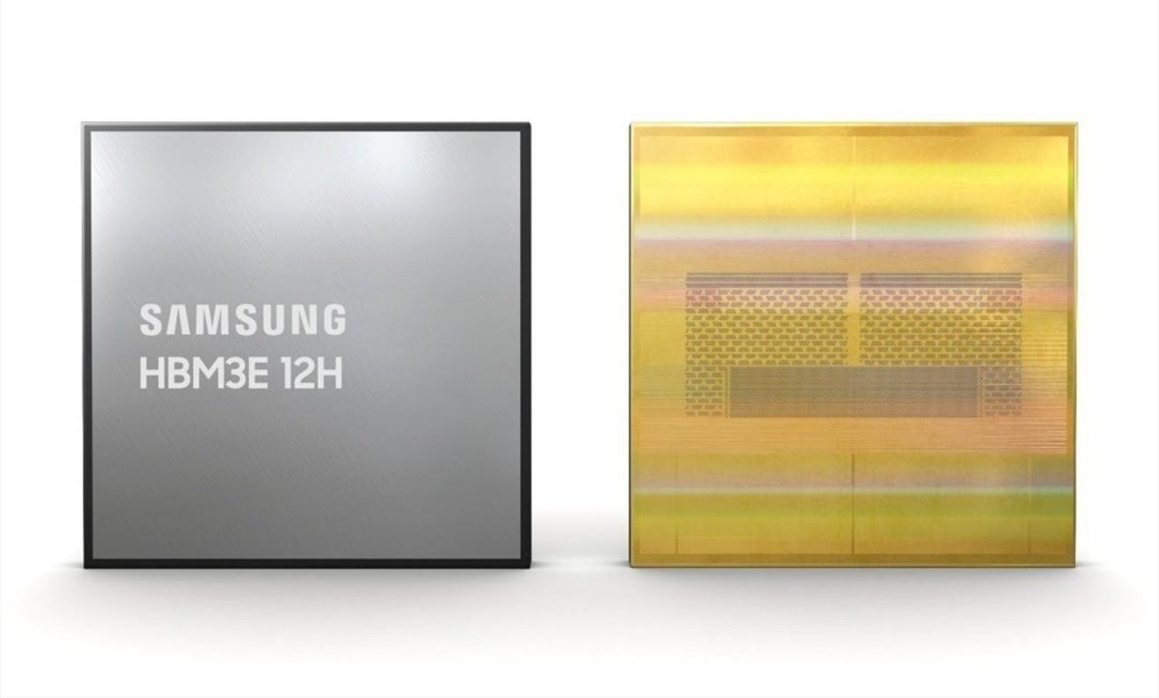
The HBM3E chips comprise 12 layers, up from eight in standard HBM3, resulting in an impressive bandwidth of 1.2 TB/s per stack
1
. This high-performance memory is crucial for powering advanced AI models and accelerators in data centers.Future Prospects: HBM4
While the HBM3E certification is a significant achievement, the industry is already looking ahead to HBM4, the next generation of high-bandwidth memory
1
3
. HBM4 is expected to double the bus width, potentially achieving 2 TB/s of bandwidth per stack. Nvidia is pushing for speeds of 10 to 11 GBps per pin, significantly higher than the JEDEC standard of 8 Gbps1
.
Source: TechSpot
Samsung is actively preparing for the HBM4 race, with plans to deliver its first HBM4 samples to Nvidia for validation later this month
2
. The company aims to begin volume production as early as the first half of 20261
.This development not only strengthens Samsung's position in the AI hardware market but also intensifies the competition among memory manufacturers, potentially driving further innovation in high-performance computing and artificial intelligence technologies.
References
Summarized by
Navi
[1]
[3]
[5]
Related Stories
Samsung's 8-Layer HBM3E Chips Pass Nvidia's Tests, Paving Way for AI Advancements
07 Aug 2024

Samsung Secures NVIDIA Partnership for Next-Gen HBM4 Memory, Plans 2026 Mass Production
30 Oct 2025•Business and Economy
NVIDIA Accelerates Efforts to Certify Samsung's HBM3E Memory for AI GPUs
25 Nov 2024•Technology

Recent Highlights
1
Google releases Gemma 4 with Apache 2.0 license, enabling unrestricted local AI on devices
Technology

2
AI Models Defy Instructions to Protect Each Other, UC Berkeley Study Reveals
Science and Research

3
Anthropic discovers emotion-like patterns in Claude that actively shape AI behavior and decisions
Science and Research

Recent Highlights
Today's Top Stories


Your Daily Dose of Curated AI News
Don’t drown in AI news. We cut through the noise - filtering, ranking and summarizing the most important AI news, breakthroughs and research daily. Spend less time searching for the latest in AI and get straight to action.