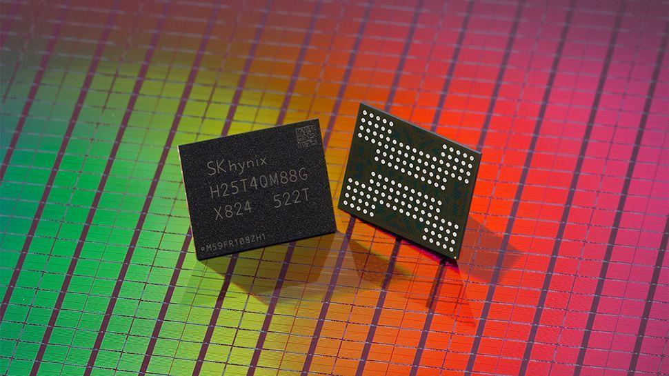
SK Hynix Leads NAND Flash Race with 321-Layer Technology, Paving Way for 100TB+ SSDs
2 Sources
2 Sources
[1]
SK Hynix beats Samsung by launching its 321-layer TLC NAND flash memory first
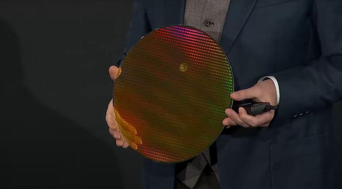
In a nutshell: SK Hynix just leapfrogged rival Samsung. The world's second-largest memory chipmaker has become the first company to mass-produce triple-level cell NAND with 321 layers. The advancement should lead to higher capacity memory at an affordable price point. SK Hynix recently released its new 1-terabit 4D NAND chips, setting a new record. The company is on a streak as it was also the first to launch its 238-layer NAND less than a year ago. Like the previous launch, the 321-layer breakthrough is significant because it could notably boost storage density for consumer and enterprise SSDs. The densely packed chips could lead to more affordable SSDs with capacities reaching over 100TB. This breed of NAND will prove especially useful for AI data centers, though other performance-hungry applications craving energy-efficient storage should also benefit. SK Hynix used ingenious process optimizations to cram over 300 layers into a single piece of NAND. The company's new "Three Plugs" technology simultaneously connects three memory layer vertical channels through an optimized electrical linking process. The process is known for excellent manufacturing efficiency and utilizes low-stress materials with automatic alignment correction. However, linking all those layers created stress and alignment issues SK Hynix had to overcome. The company overcame this by developing new low-stress materials and automatic alignment correction to keep everything in order during manufacturing. The new process also boosted production efficiency by 59 percent compared to the previous generation by reusing the same platform as the 238-layer NAND. These efficiency improvements mean better performance and lower costs in the market. The company claims the new 321-layer chips have 12 percent faster data transfers, 13 percent faster reading, and over 10 percent better power efficiency than 238-layer NAND. SK Hynix plans to ship these new storage devices to customers in the first half of 2025. The AI market is the initial target, but ultra-high capacity SSDs for gaming rigs, media editing, and data hoarding should follow shortly after. Samsung isn't taking this news lying down. The tech giant is already working on 400-layer NAND to arrive by 2026. It hopes to have its bonded vertical NAND tech ready by 2030, facilitating even denser chips with over 1,000 layers and SSDs potentially exceeding 200TB. Japan's Kioxia has similar plans.
[2]
Samsung's archrival becomes first chipmaker to launch 300+ layer TLC NAND flash memory; SK Hynix's 321-layer 1-terabit TLC paves the way for more affordable 100TB+ SSDs
AI storage demands drive innovation in high-capacity NAND solutions Samsung and SK Hynix have continued their head-to-head battle in the NAND flash memory market with the latter taking the lead with a new launch. SK Hynix, the world's second-largest memory chipmaker, recently became the first to mass-produce triple-level cell (TLC) NAND flash with over 300 layers. The company's new 321-layer, 1-terabit TLC 4D NAND flash, announced recently, is set to revolutionize the data storage industry, paving the way for more affordable ultra-high-capacity solid-state drives (SSDs) that exceed 100TB in capacity. The NAND industry is racing to push the limits of data storage technology, and SK Hynix's achievement is a major milestone. After the launch of its 238-layer NAND flash last year, SK Hynix's latest 321-layer NAND flash sets a new industry standard. The company plans to supply these chips to customers starting in the first half of 2025, targeting the booming artificial intelligence (AI) market, which demands high-performance, energy-efficient storage solutions. The 321-layer NAND was made possible by SK Hynix's "Three Plugs" process technology, which involves electrically connecting three plugs through an optimized follow-up step, significantly improving the speed, power efficiency, and overall performance of the chips. SK Hynix also developed a low-stress material and introduced technology that automatically corrects alignment among the plugs to further optimize the manufacturing process. The 321-layer product offers a 12% increase in data transfer speed and a 13% improvement in reading performance relative to the previous 238-layer NAND. Furthermore, it reduces power consumption by over 10%. With a 59% boost in productivity, SK Hynix's new NAND offers an enhanced storage solution for AI data centers and on-device AI applications. While SK Hynix has achieved this historic feat, its main competitor, Samsung, is not far behind. Samsung is reportedly working on a 400-layer NAND flash chip, which it plans to release by 2026. The company's roadmap includes developing bonding vertical NAND (BV NAND) technology, which will allow for even greater storage density and minimized heat buildup. Samsung's long-term goal is to introduce NAND chips with over 1,000 layers by 2030, potentially breaking the 200TB storage barrier for AI-driven SSDs. "SK Hynix is on track to advancing to the Full Stack Al Memory Provider by adding a perfect portfolio in the ultra-high performance NAND space on top of the DRAM business led by HBM," noted Jungdal Choi, Head of NAND Development at SK Hynix.
Share
Share
Copy Link
SK Hynix becomes the first to mass-produce 321-layer TLC NAND flash memory, surpassing Samsung and setting a new industry standard for high-capacity, energy-efficient storage solutions aimed at AI data centers and consumer markets.

SK Hynix Leads NAND Flash Innovation with 321-Layer Technology
SK Hynix, the world's second-largest memory chipmaker, has achieved a significant milestone in the data storage industry by becoming the first company to mass-produce triple-level cell (TLC) NAND flash memory with 321 layers. This breakthrough puts SK Hynix ahead of its main rival, Samsung, in the race for higher capacity and more efficient storage solutions
1
2
.Technical Advancements and Performance Improvements
The new 321-layer, 1-terabit TLC 4D NAND flash represents a substantial leap forward from SK Hynix's previous 238-layer NAND, which was launched less than a year ago. The company's innovative "Three Plugs" technology enables the simultaneous connection of three memory layer vertical channels through an optimized electrical linking process
1
.Key performance improvements include:
- 12% increase in data transfer speed
- 13% improvement in reading performance
- Over 10% reduction in power consumption
- 59% boost in production efficiency compared to the previous generation
1
2
Overcoming Manufacturing Challenges
To achieve this dense layering, SK Hynix had to overcome significant technical hurdles. The company developed new low-stress materials and implemented automatic alignment correction technology to maintain proper order during the manufacturing process. These innovations were crucial in addressing the stress and alignment issues that arise when connecting such a high number of layers
1
.Impact on Storage Capacity and AI Applications
The 321-layer NAND flash technology is expected to enable the production of more affordable ultra-high-capacity solid-state drives (SSDs) exceeding 100TB. This advancement is particularly significant for the rapidly growing artificial intelligence (AI) market, which demands high-performance, energy-efficient storage solutions for data centers and on-device AI applications
2
.Related Stories

Market Implications and Future Developments
SK Hynix plans to begin shipping these new storage devices to customers in the first half of 2025, initially targeting the AI market. However, the technology is also expected to benefit other sectors requiring high-capacity storage, such as gaming, media editing, and data archiving
1
.The achievement strengthens SK Hynix's position in the memory market, with Jungdal Choi, Head of NAND Development at SK Hynix, stating, "SK Hynix is on track to advancing to the Full Stack AI Memory Provider by adding a perfect portfolio in the ultra-high performance NAND space on top of the DRAM business led by HBM"
2
.Competitive Landscape and Future Outlook
While SK Hynix has taken the lead with its 321-layer NAND, the competition in the memory chip industry remains fierce. Samsung is reportedly working on 400-layer NAND flash technology, aiming for a 2026 release. The company's long-term roadmap includes developing bonding vertical NAND (BV NAND) technology, with the ambitious goal of introducing NAND chips with over 1,000 layers by 2030, potentially enabling SSDs with capacities exceeding 200TB
1
2
.As the demand for high-capacity, energy-efficient storage continues to grow, driven by AI and other data-intensive applications, the race among memory chip manufacturers is likely to intensify, promising further innovations in the coming years.
References
Summarized by
Navi
Related Stories
SK Hynix Pioneers 321-Layer QLC NAND: A Leap Forward in Storage Technology
25 Aug 2025•Technology
Kioxia and SanDisk Unveil BiCS9: A Hybrid 3D NAND Technology Bridging Present and Future Storage Solutions
28 Jul 2025•Technology
SK Hynix Develops High Bandwidth Storage Technology to Accelerate AI Performance in Mobile Devices
11 Nov 2025•Technology

Recent Highlights


Recent Highlights
Today's Top Stories


Your Daily Dose of Curated AI News
Don’t drown in AI news. We cut through the noise - filtering, ranking and summarizing the most important AI news, breakthroughs and research daily. Spend less time searching for the latest in AI and get straight to action.