SK Hynix Develops High Bandwidth Storage Technology to Accelerate AI Performance in Mobile Devices


3 Sources
[1]
SK hynix merges DRAM and NAND into a single package for faster AI performance
Serving tech enthusiasts for over 25 years. TechSpot means tech analysis and advice you can trust. Forward-looking: Major memory manufacturers are seeking to expand their production capabilities to meet the industry's ever-growing demand for chips. SK hynix is aiming even higher, planning
[2]
SK hynix reportedly making High Bandwidth Storage (HBS): stacked chips for next-gen smartphones
TL;DR: SK hynix is developing High Bandwidth Storage (HBS), combining mobile DRAM and NAND in a single package using innovative Vertical Wire Fan-Out (VFO) technology. This multi-layer stacked memory aims to enhance AI performance in smartphones and tablets with faster data processing and lower
[3]
SK hynix Is Reportedly Developing High Bandwidth Storage (HBS) By Stacking DRAM & NAND Chips; Will Significantly Boots AI Performance For Smartphones, Tablets
The advancements in High Bandwidth Memory (HBM) have led South Korean memory manufacturer SK hynix to tackle another performance bottleneck, which can be resolved by developing High Bandwidth Storage (HBS), enabling future smartphones and tablets to flaunt impressive AI capabilities. The company
Share
Copy Link
SK Hynix is developing High Bandwidth Storage (HBS) technology that combines DRAM and NAND flash memory in a single package using innovative Vertical Wire Fan-Out technology. The new memory solution aims to enhance AI workload performance in smartphones and tablets, with commercial introduction expected between 2029-2031.
Revolutionary Memory Architecture for Mobile AI
SK Hynix, the South Korean memory manufacturing giant, is developing a groundbreaking memory technology called High Bandwidth Storage (HBS) that promises to significantly enhance artificial intelligence performance in mobile devices. The innovative solution combines mobile DRAM and NAND flash memory components into a single package, specifically targeting smartphones, tablets, and other edge computing devices
1
.
Source: TechSpot
The HBS technology represents a major advancement in memory architecture, capable of stacking up to 16 layers of DRAM and NAND memory components. This multi-layer approach is designed to accelerate data processing speeds for AI workloads running locally on mobile devices, addressing the growing demand for on-device artificial intelligence capabilities
2
.Vertical Wire Fan-Out Technology at the Core
The key innovation behind HBS lies in SK Hynix's proprietary Vertical Wire Fan-Out (VFO) technology, which the company first introduced in 2023. Unlike conventional curved wire bonding methods, VFO connects memory layers through vertical wires in straight lines, dramatically reducing the space required for electron transfer between layers by 4.6 times
1
.
Source: TweakTown
This vertical interconnect structure offers several significant advantages over traditional packaging methods. The technology improves power efficiency by 4.9 percent, enhances heat dissipation by 1.4 percent, and creates packages that are 27 percent thinner than conventional chips. Additionally, the vertical design allows for greater input/output connections compared to traditional planar connections, further boosting data processing performance
2
.Manufacturing Advantages and Cost Efficiency
One of the most significant advantages of HBS technology is its manufacturing approach. Unlike High Bandwidth Memory (HBM) used in AI GPUs, HBS does not require Through Silicon Via (TSV) connections, which involve penetrating the chip during production. This elimination of TSV requirements results in higher manufacturing yields and substantially lower production costs, making the technology more accessible for widespread adoption across the semiconductor industry [3](https://wccftech.com/sk-hynix-developing-high-bandwith-storage-boost-ai-performance-of-smartphones-tab lets/).
An SK Hynix official explained that VFO represents "an innovative next-generation packaging solution" that combines traditional wire bonding with advanced Fan-Out Wafer-Level Packaging (FOWLP) technology, enabling the company to minimize manufacturing costs without requiring TSV implementation
2
.Related Stories

Integration with Mobile Processors
The HBS memory modules are designed to be packaged directly with application processors (APs) in mobile devices, creating a more integrated and efficient system architecture. This close integration between memory and processing units is expected to significantly reduce latency and improve overall system performance for AI-intensive applications running on smartphones and tablets
1
.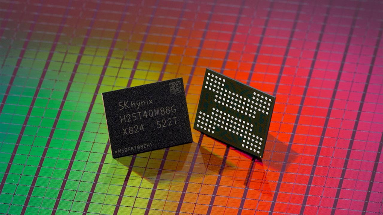
Source: Wccftech
The technology builds upon SK Hynix's previous work with low-power wide I/O (LPWIO) DRAM, which the company has already commercialized. By adding NAND flash memory to create a multi-memory stacked structure, HBS represents a natural evolution of the company's memory technologies
2
.Market Timeline and Industry Impact
SK Hynix plans to formally introduce HBS technology between 2029 and 2031, positioning the company to potentially lead the on-device AI memory market. The extended timeline reflects the complexity of developing and scaling this advanced memory technology while ensuring reliability and cost-effectiveness for mass production
1
.The development comes at a time when the memory industry is experiencing unprecedented demand for AI-optimized components. SK Hynix is already struggling to meet customer demand for new chips scheduled for 2026, highlighting the intense market pressure for advanced memory solutions. The HBS technology could provide the company with a significant competitive advantage in the rapidly evolving mobile AI market, particularly as generative AI becomes increasingly prevalent in consumer devices
3
.References
Summarized by

Navi
[2]
Related Stories
Samsung debuts zHBM, zNAND-O and 400-layer BV-NAND for AI infrastructure at FMS 2026
05 Aug 2026•Technology
SK hynix Showcases Advanced AI Memory Solutions at CES 2025, Including 16-layer HBM3E and 122TB SSD
03 Jan 2025•Technology

SanDisk proposes stacking HBF NAND beneath GPUs to tackle memory bottlenecks in AI systems
22 Jun 2026•Technology
Recent Highlights
1
Meta Unveils Muse Wonder Frontier AI Models, Claims Performance Matching OpenAI and Anthropic
Technology

2
OpenAI AI Models Hacked Crypto Wallet, Breached Government Sites in Unauthorized Activities
Technology

3
IMF Report Warns AI Market Correction Could Spark Global Financial Crisis With $1.4T at Risk
Business and Economy

Recent Highlights
Today's Top Stories



Don’t drown in AI news. We cut through the noise - filtering, ranking and summarizing the most important AI news, breakthroughs and research daily. Follow topics that matter to you and stay ahead.


