Google Pixel 11 Tensor G6 is a 3nm chip, not 2nm as previously rumored


2 Sources
[1]
Google's Tensor G6 in Pixel 11 isn't the first 2nm smartphone chip after all
It was rumored that Google's new Tensor G6, debuting in the Pixel 11, would be the first smartphone chip using TSMC's 2nm process, but it turns out that won't be the case. According to VP of Hardware at Google, Peng Yu-chun, speaking with CNA, Tensor G6 is actually produced using TSMC's 3nm
[2]
Google Pixel 11's Tensor G6 Is a 3nm Chip, Google Hardware VP Confirms
Samsung launched the world's first 2nm mobile chipset in December The Made by Google event was held earlier this week, where the Pixel 11 series was unveiled, alongside other ecosystem products. Google's latest generation flagship smartphones are powered by the proprietary Tensor G6 chipset, which
Share
Copy Link
Google confirmed its Tensor G6 chip in the Pixel 11 uses TSMC's 3nm process, not the rumored 2nm node. Despite missing the cutting-edge fabrication, the processor delivers 25% faster web browsing, 15% quicker app launches, and 50% more TPU compute power for enhanced on-device AI capabilities.

Google Confirms Tensor G6 Uses 3nm Process, Not 2nm
Google's latest Tensor G6 chip powering the Google Pixel 11 series is fabricated using TSMC's 3nm process, not the anticipated 2nm node that would have made it the industry's first 2nm smartphone chip. Peng Yu-chun, Vice President of Hardware at Google, confirmed to Taiwanese news agency CNA that the processor uses TSMC's enhanced 3nm manufacturing process
1
2
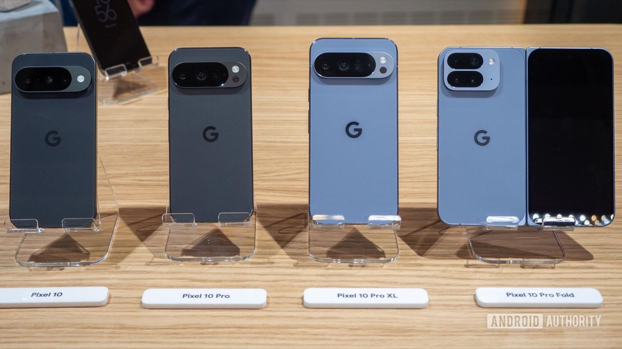
. This revelation contradicts earlier speculation suggesting Google would beat Apple to become the first smartphone manufacturer to adopt TSMC's 2nm chipmaking nodes. The Tensor G6 powers the entire Pixel 11 lineup, including the Pixel 11, Pixel 11 Pro, Pixel 11 Pro XL, and Pixel 11 Pro Fold, all unveiled at the Made by Google event earlier this week2
.Performance Upgrades Despite Missing 2nm Node
While the Tensor G6 isn't built on the cutting-edge 2nm process, Google has packed substantial performance improvements into the 3nm chip. The upgraded CPU delivers 25% faster web browsing and 15% quicker app launches compared to previous generations
1
2
. The tensor processing unit receives a significant boost with 50% more TPU compute power, enabling more sophisticated on-device AI capabilities1
2
. This enhanced TPU compute supports a new version of Gemini Nano specifically designed for on-device AI tasks, allowing the Pixel 11 to handle complex AI workloads without relying on cloud processing1
2
.Camera and Security Enhancements
The Tensor G6 features an upgraded Image Signal Processor that powers faster Night Sight processing and improved digital zoom capabilities across the Pixel 11 series
1
2
. These imaging improvements build on Google's computational photography strengths, enabling users to capture better low-light photos with reduced processing time. Security also receives attention with the upgraded Titan M3 security chip integrated into the Tensor G6 architecture1
.Related Stories

Samsung Claims 2nm Crown
Even if Google had adopted TSMC's 2nm process for the Tensor G6, it would have been the second manufacturer to launch a 2nm smartphone chip. Samsung secured that distinction in December with the Exynos 2600 SoC, the world's first 2nm node chip fabricated using advanced Gate-All-Around technology
2
. The Exynos 2600 powers the Samsung Galaxy S26 series and Galaxy Z Flip 8, combining CPU, GPU, and NPU into a single compact chip for enhanced AI and gaming experiences2
. This positions Samsung ahead in the race to smaller, more efficient chipmaking nodes, though Apple typically leads TSMC's adoption cycle for new process technologies. Watch how Google's focus on AI-specific optimizations rather than pure fabrication size impacts real-world Pixel 11 performance against competitors using more advanced nodes.References
Summarized by

Navi
Related Stories
Google's Tensor G5: A Leap Forward in AI-Powered Mobile Computing
21 Aug 2025•Technology
Google Shifts to TSMC for Tensor Chips, Aiming to Boost Pixel Performance
26 May 2025•Technology

Google Plans Lower-End Tensor G6 Chip for Pixel 11a and Pixel Tablet 3, Potentially Limiting AI Capabilities
01 Nov 2024•Technology

Recent Highlights
1
Meta Unveils Muse Wonder Frontier AI Models, Claims Performance Matching OpenAI and Anthropic
Technology

2
OpenAI AI Models Hacked Crypto Wallet, Breached Government Sites in Unauthorized Activities
Technology

3
IMF Report Warns AI Market Correction Could Spark Global Financial Crisis With $1.4T at Risk
Business and Economy

Recent Highlights
Today's Top Stories











Don’t drown in AI news. We cut through the noise - filtering, ranking and summarizing the most important AI news, breakthroughs and research daily. Follow topics that matter to you and stay ahead.


