SK hynix and SanDisk unite to standardize High Bandwidth Flash for AI inference servers
2 Sources
2 Sources
[1]
SK hynix and SanDisk announce new High Bandwidth Flash -- speedy HBF standard is targeted at inference AI servers
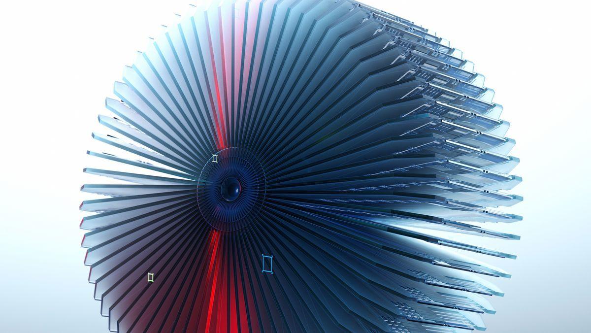
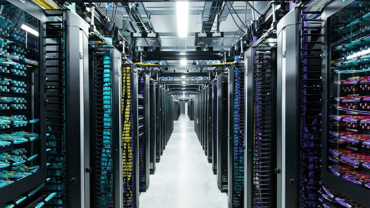
Typical NAND chips present in SSDs have steadily evolved in speed and capacity over time, with contemporary server-grade units capable of reaching 28 GB/s per unit. Somehow, that's still not enough for the AI world. In turn, SK Hynix and SanDisk have jointly announced HBF, or High Bandwidth Flash, for the inference servers of tomorrow. The official press release is exceedingly light on details, but it mentions that HBF is specifically poised to act as a layer between HBM DRAM and flash SSDs. Given that a stack of current-gen HBM3E is good for around 1.2 TB/s, we can hypothesize that HCF chips could be gunning for speeds of at least 10 GB/s each, if not more, for combined speeds in the hundreds of GB/s. After all, going to the trouble of creating an entirely new standard wouldn't make much sense otherwise. Power efficiency is apparently a concern for the standard-bearers, a pretty understandable notion in this day and age, where datacenters have massive wattage needs. A high-end Micron 9650 SSD pulls 25 W at full tilt, a figure that gets really ugly really fast when you think in exabyte-scale deployments with tens of thousands of drives. There are no specifics on how this new HBF is meant to interact with systems, but the vague wording of "supporting layer" could mean it would be analogous to an on-SSD cache, but much bigger. It could also be a really fast block storage device a la Optane that applications and/or operating systems would have to be tweaked to use efficiently. The announcement offers no target date, but it mentions that "demand of complex memory solutions, including HBF, will pick up around 2030", so that's as a good estimate as any for a production release date. The standard will be under the purview of the Open Compute Project. The companies are targeting HBF at inference servers, given that the outputs that bots users produce needs to be stored somewhere, and that storage need is projected to grow exponentially. Follow Tom's Hardware on Google News, or add us as a preferred source, to get our latest news, analysis, & reviews in your feeds.
[2]
SK hynix, Sandisk kick off standardization of HBF - The Korea Times
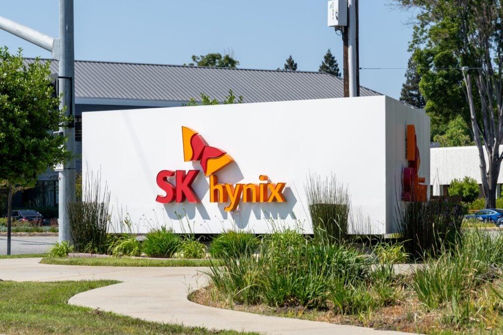
SK hynix's Icheon Campus in Gyeonggi Province / Courtesy of SK hynix SK hynix and Sandisk have teamed up for the global standardization of high-bandwidth flash (HBF), which is viewed as a new breakthrough for advancing artificial intelligence (AI) accelerators. SK hynix said Thursday it hosted a kick-off event for the HBF Spec Standardization Consortium at flash memory giant Sandisk's headquarters in Milpitas, California. The two sides will set up a dedicated team to work on HBF standardization under the Open Compute Project, the world's largest organization for sharing data center product designs and industry practices. "Together with Sandisk, we will establish HBF as an industry standard and build a foundation for the entire AI ecosystem to grow together," SK hynix said. HBF is a next-generation flash memory chip architecture for high-performance storage that will be critical for AI inference. Memory, mostly DRAM chips such as high-bandwidth memory (HBM), serves as a fast, temporary and volatile workspace for active data and applications. Storage, largely based on NAND flash memory including solid-state drives (SSDs), functions as a non-volatile repository, retaining files and apps at larger capacity but slower speeds. The importance of NAND flash has been rising rapidly in AI accelerators, as AI services increasingly shift toward inference, which requires fast and frequent access to large volumes of stored data to deliver real-time results. SK hynix said HBF will be positioned between HBM and SSDs, bridging the gap between HBM's fast performance and SSDs' storage capacity, securing both scalability and power efficiency required for AI inference. By deploying HBF, data center operators are expected to reduce total cost of ownership. Industry officials anticipate HBF could be commercialized in late 2027 or early 2028, while the demand for comprehensive memory solutions that includes HBM and HBF will fully expand around 2030. SK hynix said it will push ahead with the standardization and commercialization of HBF along with Sandisk. "Through HBF standardization, we will establish a cooperative framework and create new value by presenting an optimized memory architecture for customers and partners in the AI era," SK hynix Chief Development Officer Ahn Hyun said.
Share
Share
Copy Link
SK hynix and SanDisk have launched a joint effort to standardize High Bandwidth Flash (HBF), a next-generation flash memory architecture designed to fill the performance gap between HBM and SSDs. The new memory standard targets AI inference workloads and could reach commercialization by late 2027 or early 2028.
SK hynix SanDisk partnership targets new memory standard for AI infrastructure
SK hynix and SanDisk have kicked off a formal collaboration to establish High Bandwidth Flash (HBF) as an industry standard, addressing critical bottlenecks in AI inference servers. The two memory giants hosted an inaugural event at SanDisk's Milpitas, California headquarters to launch the HBF Spec Standardization Consortium under the Open Compute Project, the world's largest organization for sharing data center product designs
2
. This next-generation flash memory architecture aims to bridge the gap between HBM and SSDs, creating a critical middle layer for AI accelerators that demand both speed and capacity1
.High Bandwidth Flash fills critical performance void in AI inference
The importance of NAND flash has surged as AI services increasingly shift toward inference, which requires fast and frequent access to large volumes of stored data to deliver real-time results
2
. Current server-grade NAND chips can reach speeds of 28 GB/s per unit, but this falls short of what AI inference demands1
. HBF is specifically positioned as a supporting layer between HBM DRAM, which delivers around 1.2 TB/s per stack with current-gen HBM3E, and traditional flash SSDs. Industry observers speculate HBF chips could target speeds of at least 10 GB/s each, potentially achieving combined speeds in the hundreds of GB/s1
. This architecture could function similarly to an expanded on-SSD cache or as a fast block storage device comparable to Optane, though applications and operating systems may need optimization to use it efficiently.Power-efficient storage solutions address datacenter energy challenges
Power efficiency stands as a core design principle for HBF standardization, reflecting urgent concerns about datacenter energy consumption. High-end SSDs like the Micron 9650 consume 25 W at full capacity, a figure that scales alarmingly when considering exabyte-scale deployments with tens of thousands of drives
1
. By securing both scalability and power efficiency required for AI inference, HBF aims to help data centers reduce total cost of ownership2
. SK hynix Chief Development Officer Ahn Hyun emphasized that "through HBF standardization, we will establish a cooperative framework and create new value by presenting an optimized memory architecture for customers and partners in the AI era"2
.Related Stories

Timeline and market implications for memory solutions
Industry officials anticipate HBF could be commercialized in late 2027 or early 2028, while demand for comprehensive memory solutions that include HBM and HBF will fully expand around 2030
2
. The companies are establishing a dedicated team to work on HBF standardization, with SK hynix stating they will "establish HBF as an industry standard and build a foundation for the entire AI ecosystem to grow together"2
. The standard specifically targets AI inference servers, where outputs that users produce need storage, and that storage need is projected to grow exponentially1
. This positions HBF to enhance AI accelerators by providing the storage capacity and bandwidth balance that current memory architectures struggle to deliver efficiently.References
Summarized by
Navi
[1]
Related Stories
SK Hynix Develops High Bandwidth Storage Technology to Accelerate AI Performance in Mobile Devices
11 Nov 2025•Technology

Nvidia and SK Hynix develop AI SSD targeting 100 million IOPS to solve inference bottlenecks
17 Dec 2025•Technology
SK hynix Showcases Advanced AI Memory Solutions at CES 2025, Including 16-layer HBM3E and 122TB SSD
03 Jan 2025•Technology

Recent Highlights


Recent Highlights
Today's Top Stories


Your Daily Dose of Curated AI News
Don’t drown in AI news. We cut through the noise - filtering, ranking and summarizing the most important AI news, breakthroughs and research daily. Spend less time searching for the latest in AI and get straight to action.