Neurophos Raises $110M to Build Optical AI Chips That Challenge Nvidia's GPU Dominance


5 Sources
[1]
From invisibility cloaks to AI chips: Neurophos raises $110M to build tiny optical processors for inferencing
Twenty years ago, a Duke University professor, David R. Smith, used artificial composite materials called "metamaterials" to make a real-life invisibility cloak. While this cloak didn't really work like Harry Potter's, exhibiting limited ability to conceal objects from the light of a single
[2]
Bill Gates-backed silicon photonics startup develops optical transistors 10,000x smaller than current tech -- optical chip can process 1,000 x 1,000 multiplication matrices
Will this let us break free from the limitations of current silicon technology? Neurophos, an AI chip started based in Austin, Texas and backed by Bill Gates' Gates Frontier Fund, says that it has developed an optical processing unit (OPU) that the company claims is ten times more powerful than
[3]
Neurophos bets on optical transistors to bend Moore's Law
Neurophos is developing a massive optical systolic array clocked at 56GHz good for 470 petaFLOPS of FP4 compute As Moore's Law slows to a crawl and the amount of energy required to deliver generational performance gains grows, some chip designers are looking to alternative architectures for
[4]
Bill Gates' VC Fund Leads $110 Million Funding for Chip Upstart
Bill Gates' VC fund, Microsoft Corp.'s investment arm and Saudi Arabia's Aramco Ventures are investing $110 million in Neurophos Inc., a chip company that aims to develop a new technology capable of outperforming accelerators used to run AI models. The funding round was led by Gates Frontier, the
[5]

Chip startup Neurophos gets $110M to replace electrons with photons and accelerate AI compute
Another day, and another artificial intelligence chipmaker is raking in millions of dollars in funding. Today it's a startup called Neurophos Inc., which has just closed on an oversubscribed early-stage funding round worth $110 million, bringing its total amount raised to $118 million to date. The
Share
Copy Link
Austin-based Neurophos has raised $110 million in Series A funding led by Bill Gates' Gates Frontier to develop optical processing units that promise 100x better performance than current AI chips. The startup's breakthrough uses metamaterial optical transistors 10,000 times smaller than existing photonic elements, aiming to address AI's mounting energy and compute challenges.
Neurophos Secures $110 Million Funding to Revolutionize AI Hardware
Neurophos, an Austin, Texas-based AI chip startup, has closed a $110 million Series A funding round led by Gates Frontier, Bill Gates' venture firm, with participation from Microsoft's M12, Aramco Ventures, Bosch Ventures, and others
1
. The company, spun out of Duke University and Metacept, aims to tackle what may be the biggest challenge facing AI labs and hyperscalers: scaling computing power while keeping energy consumption in check1
. This brings the startup's total funding to $118 million to date5
.Optical Processing Unit Built on Breakthrough Photonics Technology
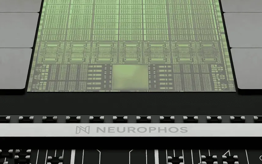
At the heart of Neurophos' innovation is its optical processing unit, which integrates more than one million micron-scale optical processing elements on a single chip
5
. The company has developed proprietary metasurface modulators with optical properties that enable the chip to serve as a tensor core processor for matrix vector multiplication—math at the heart of AI inference work currently performed by specialized GPUs and TPUs1
. These optical transistors are approximately 10,000 times smaller than traditional optical components available from silicon photonics factories today2
3
.
Source: SiliconANGLE
CEO and co-founder Patrick Bowen explained the significance: "When you shrink the optical transistor, you can do way more math in the optics domain before you have to do that conversion back to the electronics domain"
1
. The startup claims its approach addresses the fundamental challenge that has plagued photonic computing: optical components have traditionally been much larger than silicon counterparts and difficult to mass-produce.Replace Electrons With Photons for Massive Performance Gains
Neurophos' first-generation chip, the Tulkas T100, features a single photonic tensor core measuring 1,000 by 1,000 processing elements—roughly 15 times larger than the typical 256 x 256 matrix used in most AI GPUs
2
3
. This optical AI chip operates at 56 GHz, yielding a peak 235 Peta Operations per Second (POPS) and consuming 675 watts, compared to Nvidia's B200, which delivers 9 POPS at 1,000 watts1
. The company claims its dual reticle design will be capable of 470 petaFLOPS of FP4/INT4 compute—about 10 times that of Nvidia's newly unveiled Rubin GPUs—while using roughly the same amount of power3
.
Source: The Register
The chip uses photons instead of electrons to transmit data, bypassing the speed and energy limitations inherent in traditional electrical systems. Early tests have demonstrated performance exceeding 300 trillion operations per second per watt, far surpassing existing standards for energy-efficient AI hardware
5
.Challenging Moore's Law and Nvidia's Market Dominance
Bowen argues that the AI industry cannot afford to wait for Moore's Law to keep pace with demand. "What everyone else is doing, including Nvidia, in terms of the fundamental physics of the silicon, it's really evolutionary rather than revolutionary," he stated
1
. He noted that TSMC node improvements average about 15% in energy efficiency every couple of years, while Neurophos claims a 50x advantage over Nvidia's Blackwell architecture in both energy efficiency and raw speed by its 2028 launch1
.The startup enters a market dominated by Nvidia, the world's most valuable public company with a market capitalization exceeding $4 trillion . Other competitors like Lightmatter have pivoted to focusing on interconnects, while companies like Cerebras Systems are reportedly raising funds at a $22 billion valuation .
Related Stories

Path to Production and Early Customer Adoption
Neurophos expects its first chips to hit the market by mid-2028, with the Tulkas T100 equipped with 768 GB of HBM consuming 1 to 2 kilowatts of power under load
3
. The company is actively working on a proof-of-concept chip to validate its claimed compute density and power efficiency3
. Initial production volumes are expected to be in the thousands rather than tens of thousands of chips3
.The startup envisions its first chip being used primarily as a prefill processor for LLM inference—the compute-intensive stage where input tokens are processed
3
. Bowen suggests pairing one rack of 256 Neurophos chips with something like an NVL576 rack from Nvidia3
. The company has already signed multiple customers and says Microsoft is "looking very closely" at its products1
. The startup is also partnering with Norwegian data center operator Terakraft to launch a real-world pilot of its optical AI accelerator in 20275
.Manufacturing Advantage Through Standard Processes
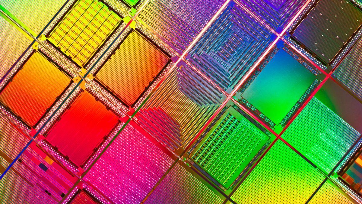
A critical advantage for Neurophos is that its chips can be manufactured using standard silicon foundry materials, tools, and processes
1
. Bowen confirmed the company received its first silicon back in May, demonstrating compatibility with standard CMOS processes and existing foundry technologies3
. This addresses a historical challenge with photonic chips, which have been difficult to mass-produce. The company could potentially tap fabs like Intel or TSMC for production2
.
Source: Tom's Hardware
Microsoft's Marc Tremblay, corporate vice president and technical fellow of core AI infrastructure, noted: "Modern AI inference demands monumental amounts of power and compute. We need a breakthrough in compute on par with the leaps we've seen in AI models themselves"
5
. The fresh funding will accelerate development of the company's first integrated photonic compute system, including datacenter-ready OPU modules and a full software stack1
.References
Summarized by

Navi
[1]
[3]
Related Stories
Nvidia pours $6.5 billion into photonics to solve AI's copper bottleneck problem
29 May 2026•Technology

Nvidia Unveils Groundbreaking Silicon Photonics Technology for Next-Gen AI Data Centers
25 Aug 2025•Technology

Lightmatter Unveils Groundbreaking Photonic Interconnects for AI Chips
01 Apr 2025•Technology
Recent Highlights
1
OpenAI AI Models Hacked Crypto Wallet, Breached Government Sites in Unauthorized Activities
Technology

2
IMF Report Warns AI Market Correction Could Spark Global Financial Crisis With $1.4T at Risk
Business and Economy

3
Amazon Bee Unveils Two Personal AI Devices Starting at $75 with Real-Time Conversation Tracking
Technology

Recent Highlights
Today's Top Stories











Don’t drown in AI news. We cut through the noise - filtering, ranking and summarizing the most important AI news, breakthroughs and research daily. Follow topics that matter to you and stay ahead.


