3 Sources
[1]
Nvidia custom 'NVHBM' promises 30% higher bandwidth, 15% lower power than commodity HBM4e -- custom base die and PHY will be available to NVLink Fusion partners
Nvidia's NVLink Fusion program gives the company's partners the building blocks necessary to connect custom chips with the NVLink scale-up domain used to join many separate processors into a single coherent system like the Vera Rubin NVL72 rack-scale accelerator. Today, Nvidia is adding a new building block to that toolkit: NVHBM, a custom implementation of the high-bandwidth memory that underpins practically every AI accelerator in use today. As Nvidia describes it, NVHBM is a custom HBM base die that promises higher bandwidth, lower power usage, and a smaller on-die footprint than traditional HBM4e. Nvidia says it's designed and validated with "leading memory vendors," so it promises custom silicon developers faster time-to-market than implementing commodity HBM from the ground up. But it's worth re-emphasizing that this isn't an HBM replacement. Instead, it's a new building block that Nvidia is only offering to its custom silicon partners. Memory bandwidth is everything for AI accelerators, and NVHBM promises up to 30% higher bandwidth per stack than standard HBM4e. For memory-bandwidth-bound AI workloads, that higher bandwidth translates into higher throughput, such as a higher tokens-per-second rate for AI inference. The custom NVHBM base die also reduces the footprint of memory-related circuitry on the main custom accelerator die. Traditionally, the HBM memory controller has been incorporated into the primary silicon die on the package. NVHBM instead moves the memory controller into the base die of the HBM stack and provides a smaller custom PHY that NVLink Fusion customers can then integrate into their designs. Nvidia says this approach frees up precious package real estate that can then be used for additional compute die area -- up to 30% more compute on the primary silicon die. NVHBM further promises to simplify the interposer routing used to join multiple chips together for designs using advanced packaging techniques. NVHBM also provides power savings versus off-the-shelf HBM4e stacks. As Nvidia has continuously hammered home in the Vera Rubin roll-out, every watt that isn't going into token production is a watt wasted. Nvidia says NVHBM uses 15% less power than commodity HBM4e, and that power savings can be banked for performance-per-watt improvements, reallocated into more functional units for a custom accelerator design, or translated into higher sustained performance within the same power budget. Higher bandwidth at lower power is a huge win for AI accelerators that are moving massive data structures like model weights and KV caches around, especially when those savings are multiplied across many thousands of chips. The energy saved on data movement can be plowed back into higher performance from the accelerator itself or reallocated to support larger numbers of accelerators within the same fixed power envelope. But these are, as of now, reasons for Nvidia's prospective partners to consider incorporating NVLink Fusion and NVHBM into their custom designs, not benefits that will materialize in the Rubin rack-scale systems already in production. Along with NVHBM itself, Nvidia announced that Amazon's Annapurna Labs will be its first partner on NVHBM. , and Annapurna VP Nafea Bshara says: "We look forward to this technology collaboration to benefit future AWS infrastructure designs." Annapurna's next-generation Trainium 4 AI chips will already support the NVLink Fusion scale-up interface, so it seems likely that follow-on chips will support NVHBM, too. Follow Tom's Hardware on Google News, or add us as a preferred source, to get our latest news, analysis, & reviews in your feeds.
[2]
NVIDIA NVLink Fusion Expands With NVHBM Custom High-Bandwidth Memory
Amazon's Annapurna Labs will be the first to collaborate on NVHBM technology alongside NVLink Fusion. The next wave of AI is placing new demands on infrastructure. As AI agents and trillion-parameter workloads become mainstream, the performance of AI infrastructure depends not only on compute, but on how compute, memory, storage, networking and software are designed together as a unified system. To help hyperscalers and AI innovators build the next generation of semi-custom AI infrastructure, NVIDIA today expanded NVIDIA NVLink Fusion with NVIDIA NVHBM, a next-generation high-bandwidth memory technology that brings higher memory performance and efficiency to XPUs. It will be validated and offered by leading memory partners, extending this advanced memory capability to NVLink Fusion customers. Traditional HBM architectures place the memory controller on the XPU die, consuming valuable silicon area that could otherwise be dedicated to compute. NVHBM, built on the same technology that NVIDIA will use for future GPUs, integrates NVIDIA's custom memory controller into the HBM base die. By integrating the memory controller into the 3D HBM stack instead of the XPU, NVHBM delivers up to 30% greater memory bandwidth and 15% lower HBM power consumption, and frees up to 25% more area on XPU compute die compared with standard HBM4E. NVIDIA is establishing a standard NVHBM implementation, available from multiple memory providers. This reduces the engineering effort required to integrate and qualify memory across multiple suppliers -- giving NVLink Fusion customers a faster path for bringing custom AI chips to market. Amazon's Annapurna Labs will be the first to work on NVHBM as part of its broader collaboration with NVIDIA around NVLink Fusion. AWS and NVIDIA Continue NVLink Fusion Collaboration Amazon's Annapurna Labs will work with NVIDIA on NVHBM technology and the NVLink scale-up architecture to enhance performance and efficiency for AI workloads. This builds on AWS's previously announced support for NVLink Fusion. Annapurna Labs will support NVLink Fusion with its next-generation Trainium chips starting with Trainium4, which would allow Amazon chips and NVIDIA GPUs to work together with common rack-scale architecture. "NVHBM represents a new architectural approach to advancing high-bandwidth memory performance and efficiency," said Nafea Bshara, vice president of Annapurna Labs at Amazon. "We look forward to this technology collaboration to benefit future AWS infrastructure designs." Vertically Integrated and Horizontally Open NVLink Fusion enables partners to connect custom XPUs and CPUs to NVIDIA's rack-scale platform. Partners can access NVIDIA NVLink chiplets, NVLink-C2C, NVLink Switches and NVIDIA MGX systems and racks, as well as a broad ecosystem of CPU partners, ASIC designers, system manufacturers and technology providers. Offered with each generation of NVIDIA's rack-scale system architecture, NVLink Fusion allows hyperscalers and AI-native companies to focus engineering resources on XPU innovation while using a proven technology stack for scale-up and scale-out networking, rack-scale systems and software -- creating a faster, lower-risk path to deploying semi-custom AI infrastructure. Learn more about NVLink and NVLink Fusion.
[3]
NVIDIA Develops Custom "NVHBM" Memory For AI, Claiming 30% More Bandwidth and 15% Lower Power Than HBM4E
NVIDIA has just announced its custom HBM solution called NVHBM, which will be used in future GPUs, offering higher bandwidth & lower power. NVHBM Is A Custom HBM Solution Designed By NVIDIA & Amazon's Annapurna Labs To Speed Up DRAM Capabilities For Future Agentic & Physical AI Workloads The NVIDIA NVHBM DRAM solution is an extension of NVLink Fusion, offering higher memory performance and efficiency to XPUs at a time when memory bandwidth is becoming critical as model sizes increase tremendously into the trillion-parameter era. NVIDIA says that its NVHBM solution offers better bandwidth and efficiency than standard HBM solutions by taking the memory controller off of the XPU and placing it directly within the base die of HBM. We have seen many memory vendors and chipmakers working on similar solutions. This technology will be incorporated into future GPUs, and the memory controller itself will be a custom design by NVIDIA, which will be integrated within the HBM base die. Through this solution, it is said that the memory bandwidth will see a 30+% boost while power consumption will be 15% lower than a standard HBM4E solution. Removing the memory controller from the XPU also saves up to 25% die area on the main chip, which can be dedicated to additional compute capabilities. Table 1. NVHBM brings three main platform-level advantages to AI accelerator programs: higher memory bandwidth, more package and silicon area, and lower HBM power usage As for adoption, NVIDIA is establishing a standard NVHBM implementation which will be available from multiple memory providers. This will help reduce the engineering effort that will otherwise be required for the integration and qualification of the memory design across multiple suppliers. Those part of the NVLink Fusion ecosystem will also be able to bring custom AI chips to market faster. "NVHBM represents a new architectural approach to advancing high-bandwidth memory performance and efficiency," said Nafea Bshara, vice president of Annapurna Labs at Amazon. "We look forward to this technology collaboration to benefit future AWS infrastructure designs." One of the first partners that will utilize NVIDIA NVHBM is Amazon's Annapurna Labs, which will work together towards the integration of NVHBM technology and the NVLink scale-up architecture for enhanced performance and efficiency across AI workloads. The next-gen AWS Trainium chips, starting with Trainium4, will use NVLink Fusion to connect NVIDIA GPUs with Amazon chips under a common rack-scale architecture. Since NVIDIA has already mentioned custom HBM for its Feynman GPUs, we can expect the generation to be the first to adopt NVHBM when it launches in 2028. Follow Wccftech on Google to get more of our news coverage in your feeds.
Share
Copy Link
Nvidia has introduced NVHBM, a custom high-bandwidth memory solution that promises 30% higher bandwidth and 15% lower power consumption than standard HBM4e. The technology moves the memory controller into the HBM base die, freeing up to 25% more die area for compute. Amazon's Annapurna Labs will be the first partner to adopt NVHBM for future AWS infrastructure designs.
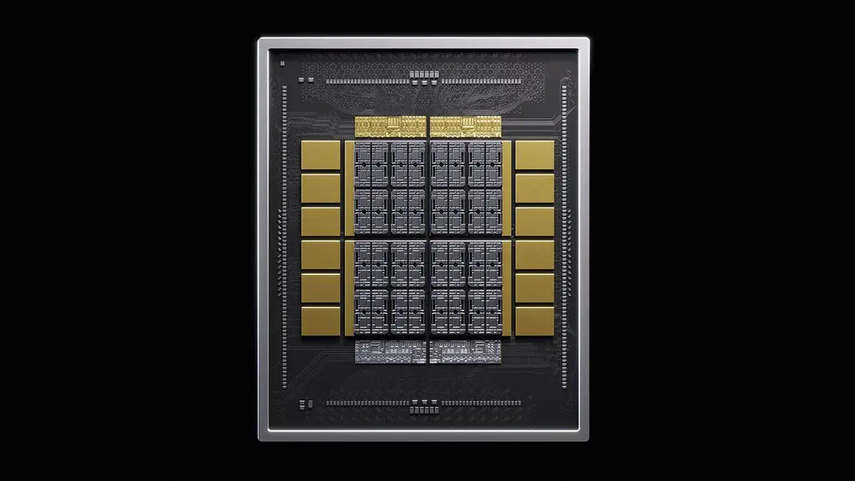
Nvidia has announced NVHBM, a custom high-bandwidth memory solution designed to address the escalating demands of AI infrastructure as trillion-parameter workloads and AI agents become mainstream
1
2
. The technology represents an expansion of the NVLink Fusion program, which provides partners with building blocks to connect custom chips within Nvidia's rack-scale platform architecture2
. NVHBM delivers 30% higher bandwidth per stack compared to standard HBM4e, directly translating to higher tokens-per-second rates for AI inference workloads that are memory-bandwidth-bound1
3
.Traditional HBM architectures incorporate the memory controller into the primary silicon die on the package, consuming valuable real estate that could be dedicated to compute functions
2
. NVHBM fundamentally changes this approach by integrating Nvidia's custom memory controller directly into the base die of the 3D HBM stack1
3
. This architectural shift frees up to 25% more area on XPU compute dies, allowing designers to add up to 30% more compute capabilities on the primary silicon die1
2
. The technology also simplifies interposer routing used to join multiple chips together in designs using advanced packaging techniques1
.NVHBM achieves 15% lower power consumption compared to commodity HBM4e, addressing a critical concern for AI infrastructure operators
1
2
. These power savings can be reallocated into more functional units for custom AI chip designs, translated into higher sustained performance within the same power budget, or banked for improved performance-per-watt metrics1
. For hyperscalers deploying thousands of AI accelerators, these savings multiply significantly when moving massive data structures like model weights and KV caches1
. The energy saved on data movement can support larger numbers of accelerators within the same fixed power envelope1
.Related Stories
Amazon's Annapurna Labs will be the first partner to collaborate on NVHBM technology as part of its broader work with Nvidia around NVLink Fusion
2
3
. Nafea Bshara, vice president of Annapurna Labs at Amazon, stated that "NVHBM represents a new architectural approach to advancing high-bandwidth memory performance and efficiency" and expressed anticipation for how "this technology collaboration to benefit future AWS infrastructure designs"2
3
. Annapurna's next-generation Trainium 4 chips will support NVLink Fusion, allowing Amazon chips and Nvidia GPUs to work together within a common rack-scale architecture1
2
.Nvidia is establishing a standard NVHBM implementation that will be validated and offered by leading memory vendors, reducing the engineering effort required to integrate and qualify memory across multiple suppliers
2
3
. This standardization provides NVLink Fusion customers with a faster path for bringing custom AI chips to market compared to implementing commodity HBM from the ground up1
2
. The technology will be available exclusively to Nvidia's custom silicon partners through the NVLink Fusion program, which also provides access to NVLink chiplets, NVLink-C2C, NVLink Switches, and Nvidia MGX systems and racks2
. Nvidia has indicated that NVHBM will be incorporated into future GPUs, with speculation pointing to the Feynman GPU generation expected in 2028 as a potential first adopter3
.Summarized by
Navi
[1]
19 Mar 2025•Technology

11 Dec 2024•Technology

10 Feb 2026•Technology

1
Technology

2
Technology

3
Policy and Regulation