Qualcomm unveils High-Bandwidth Compute architecture to break AI memory wall with 6x efficiency
4 Sources
[1]
Qualcomm reveals HBC near-memory AI architecture, AI250 and AI350 accelerators -- touts 6x higher bandwidth-per-watt compared to HBM, 200x capacity compared to on-chip SRAM
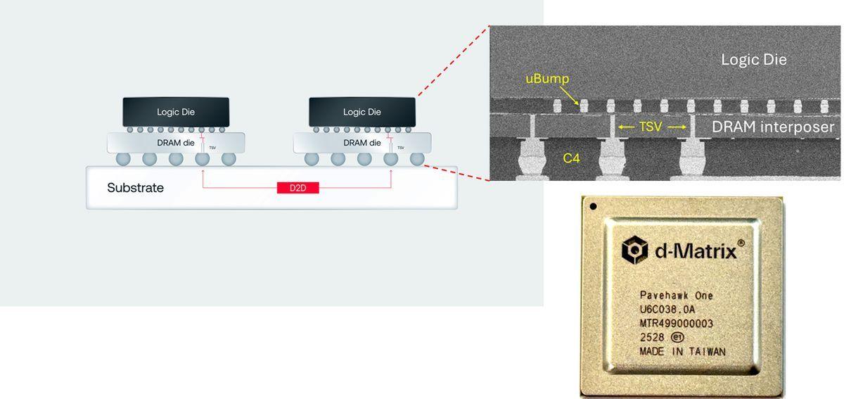
The so-called memory wall is a major performance limiter for many AI workloads, and high bandwidth memory (HBM) is not always a panacea since compute capability is growing faster than memory bandwidth. Qualcomm on Wednesday introduced its HBC near-memory compute architecture called high-bandwidth compute (HBC) that is designed to break the memory wall and enable the performance of certain AI workloads to scale linearly. Qualcomm's approach to near-memory compute is pretty much straightforward: the company disaggregates the AI accelerator from the system-on-chip (SoC) and puts it under the LPDDR DRAM stack. The HBC accelerator connects to the LPDDR stack using through-silicon vias to provide maximum bandwidth and capacity without using expensive HBM memory and advanced packaging. Qualcomm does not disclose the actual bandwidth HBC provides, though the company claims that it offers 6X higher bandwidth-per-watt compared to HBM and over 200X capacity compared to on-chip SRAM. "We have separated the AI accelerator from the XPU and placed the XPU directly beneath a DRAM stack," said Tony Pialis, Executive Vice President and General Manager of Data Center Business at Qualcomm. "This is very important because it gives us the performance advantages of SRAM with the density and capacity of stacked memory. In effect, the congestion associated with HBM is gone. The value to the industry is lower power consumption, less heat, and the elimination of the costly silicon interposer used by HBM solutions. We can also deploy multiple HBC stacks within a single compute device using standard packaging, which delivers a significant performance-per-cost advantage." Putting DRAM on logic or next to logic is nothing new. All DRAM makers have experimented with near-memory compute architectures, but have failed to make them popular. More recently, GUC, a fabless ASIC design service company, proposed its DRAM-on-Logic (DoL) technology that places one to four DRAM layers on top of logic to get around 5 TB/s of memory bandwidth and offer higher performance than some HBM3E memory subsystems without using expensive advanced packaging and HBM3E stacks. Since Qualcomm does not disclose actual performance numbers, it is hard to compare its HBC to GUC's offering. However, the biggest caveat about HBC is that Qualcomm does not tell us what the HBC accelerator actually does. In theory, it could be everything: a transformer-specific near-memory engine, a more general array of tensor cores, or some kind of preprocessing logic for AI inference or training. Along with its HBC technology, Qualcomm also disclosed its HBC roadmap. While the company's AI200 accelerator, due later this year, will rely on LPDDR5X and offer 43 TB of RAM per rack, its successor AI250 will rely on the 1 Generation HBC that will offer 18X bandwidth of AI200. The AI300 will use 2 Generation HBC that will provide 54X bandwidth of AI300. Follow Tom's Hardware on Google News, or add us as a preferred source, to get our latest news, analysis, & reviews in your feeds.
[2]
Qualcomm's proposed solution to catch up in AI infra: Bury the compute under the DRAM
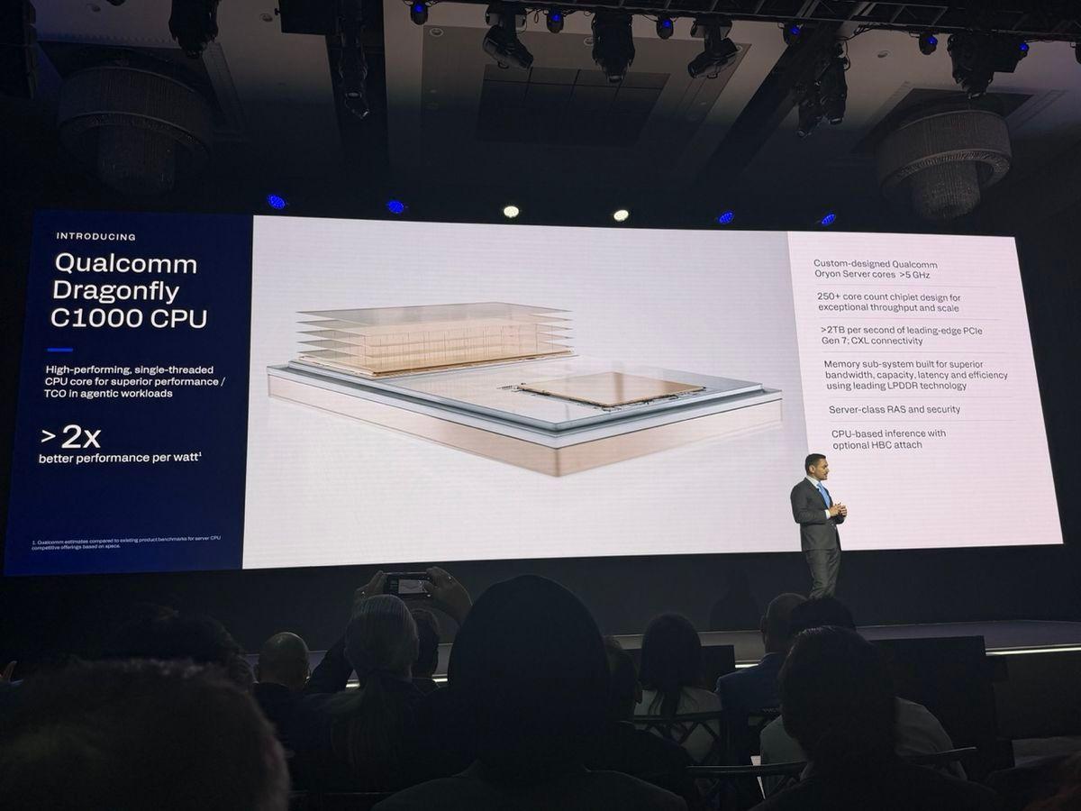
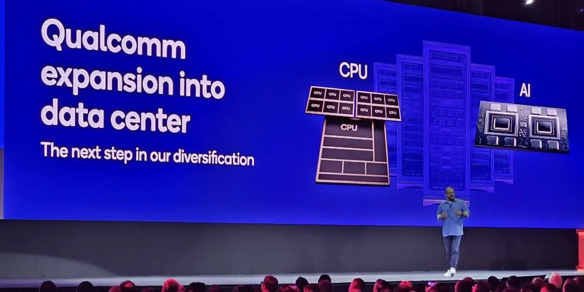
Qualcomm is finally getting serious about AI infrastructure, but its push into the datacenter hinges on the success of an ambitious near-memory compute architecture designed to deliver better inference economics than today's GPUs. Announced during its 2026 investor day last week, the tech will see Qualcomm stack layer upon layer of DRAM on top of its XPUs to form a single unified compute and memory module it's calling high-bandwidth compute (HBC). "We offer all of the performance advantages of SRAM, but with the density and the memory capacity that HBM (high-bandwidth memory) stacks offer," Tony Pialis, Qualcomm's EVP of datacenter, claimed during last week's investor presentation. This technology is set to launch next year as part of Qualcomm's AI250-series of Dragonfly rack systems, and marks a distinct shift in Qualcomm's AI infrastructure strategy. The handset giant is no stranger to AI accelerators. Essentially every Snapdragon processor sold today ships with an NPU on board. But in the datacenter, the company has struggled to garner the same excitement as Nvidia, AMD, and even startups like Cerebras. Compared to the big two's GPUs, Qualcomm's AI-series accelerators haven't compared that favorably, but that could soon change as the company looks to make its mark on the datacenter. With the AI250, the SoC maker is claiming 768 GB of memory capacity and up to 133 TB/s of effective memory bandwidth per card. For reference, Nvidia's Groq 3 LPUs offer just 500 MB of SRAM and 150 TB/s of bandwidth. If that seems too good to be true, that's because it is. Qualcomm is leaning heavily on the word "effective." We know that because for the AI200-based Dragonfly systems rolling out this year, they claimed 414 TB/s of "effective" memory bandwidth across all 56 chips. On its face, that seems more realistic, but actually achieving that with 8800 MT/s LPDDR5x alone would require a 6,720-bit-wide bus, which it almost certainly does not possess. Qualcomm insists that this is the "pure physical bandwidth of the LPDDR interface," but declined to offer any specifics as to how it's somehow managed to achieve what Nvidia needed eight HBM3e stacks to do. In any case, according to Qualcomm's marketing materials, with the move to HBC, the AI250 will offer 18x the effective bandwidth of the AI200, while the forthcoming AI300 will deliver 54x the bandwidth. Given the context, these seem like outlandish claims, but these "effective" multipliers are really a feature of Qualcomm's HBC architecture. Unpacking high-bandwidth compute Amplifying "effective" bandwidth isn't the only party trick from these HBC-based accelerators. Qualcomm claims that by moving some of the XPU's compute under the DRAM, it can significantly reduce the amount of power its chips consume. On a conventional datacenter GPU, data is rapidly shuffled between HBM and the compute dies. Even using advanced packaging technologies like TSMC's CoWoS, the power required to move this data back and forth is significant. By stacking the DRAM directly on top of some of the logic and connecting them using through-silicon vias (TSVs), the path from compute to memory is shortened considerably. "Imagine working in the same building that you live in so you only travel up and down," Pialis said. "What does that mean for the highways and the roads that connect the suburbs to the city? Guess what? The roads are clear. The value this brings to the industry is lower power consumption, less heat, and that expensive road of silicon interposer that HBM solutions use is no longer needed." Performing bandwidth-bound operations on the base die also has the benefit of reducing the amount of data that needs to be shuttled to and from the HBC to the SoC. In effect, memory bandwidth is amplified. This is why Qualcomm is using "effective bandwidth" so liberally. Compared to doing all of that work on a conventional GPU or XPU with distinct HBM and compute dies, the effective bandwidth would be significantly higher, which also achieves better density than SRAM-only designs, like Nvidia's LPUs or Cerebras' dinner plate sized accelerators. With that said, Qualcomm probably won't be running its entire AI software stack on HBC. Higher memory bandwidth primarily benefits decode, when the entirety of the model's active weights are streamed autoregressively from memory one token after another. Decode isn't particularly compute-intensive. As such, doing decode partially or entirely in HBC starts to make a lot of sense because it also avoids the thermal constraints associated with burying the compute under multiple layers of DRAM. Qualcomm tells us that the AI250 can be used as a standalone AI accelerator, but notes it is heavily optimized around addressing bandwidth bottlenecks. So, in addition to being a dedicated inference chip, it can be used in disaggregated inference architectures that use GPUs or other Qualcomm parts for prompt processing and the AI250 to speed up memory intensive decode operations. Peak FLOPS are notably missing from Qualcomm's AI250 disclosures -- the company declined to share specifics upon our request. Is HBC actually a competitive advantage? While Qualcomm is early among chip designers to make a fuss about near-memory or HBC, it's not the first, nor is the technology beyond the means of Nvidia or AMD. In fact, both Nvidia and AMD are rumored to be working with HBM suppliers and TSMC to develop custom base dies to boost the performance of their next-gen chips, though it's still not clear how much, if any, compute has been integrated into them. Qualcomm tells us its HBC "uses LPDDR memory in a purpose-built near-memory computing architecture that combines compute and highly-accelerated memory bandwidth within a 3D-stacked silicon design. While both HBC and HBM use stacked-memory concepts, HBC is a distinct architecture designed to address AI's data-movement bottleneck by bringing compute and memory closer together, increasing memory bandwidth efficiency and improving energy efficiency for AI inference workloads. HBM has more stacks of DRAM, uses 2.5D interposer to route more wires, and does not do computing in the base logic die." AI chip startup d-Matrix is also developing accelerators that will use 3D stacked DRAM to extend their in-memory compute capabilities. The underlying technology described by Pialis may not be as unique as Qualcomm would like investors to believe, but it shows the company hasn't missed the boat. However, Qualcomm's ability to work with Nvidia and AMD may end up doing more to sell customers on its tech than anything. As we previously wrote, in a disaggregated AI world, Nvidia can be both a friend and an enemy. Qualcomm finds its Mojo In addition to teasing its upcoming AI250 and AI300 accelerators, Qualcomm's investor day also coincided with the acquisition of AI software startup Modular. Modular was founded by Tim Davis and Chris Lattner, the latter of whom you may recognize as the creator of LLVM, Clang, the Swift programming language, and the multi-level intermediate representation (MLIR) compiler infrastructure. At Modular, Lattner and crew developed Mojo, a low-level programming interface for GPUs, which offered a high-performance alternative to Nvidia's CUDA or AMD's HIP and ROCm stacks. The big idea is that users should be able to write highly performant AI apps that'll run regardless of the underlying hardware. For Qualcomm, Mojo presents an opportunity to sidestep the CUDA moat, which has dogged AMD for so long. With Mojo, Qualcomm's customers won't need to choose one platform; they can develop their apps and run them on whatever compute is handy at the time. It's not all or nothing either. Modular should help to support heterogeneous deployments similar to what Nvidia is doing with Groq's LPU tech, where GPUs might be used for prefill and AI250s are used for decode in whatever ratio makes the most sense for that specific application. However, the acquisition doesn't just buy Qualcomm a vendor-neutral programming model. The folks buying these systems are primarily concerned with one AI workload in particular: LLM model serving. For this, Modular developed a serving platform called Max. Max is a bit like SGLang or vLLM in that it'll run interchangeably on AMD or Nvidia hardware, but because it's built atop Mojo, it, at least in theory, shouldn't require nearly as much hand tuning. The offering should help Qualcomm compete in a landscape where software has become even more important than the hardware it runs on, if it manages to close the acquisition this year without regulators stepping in. In any case, we won't have to wait much longer to see the HBC in action. After launching its AI200-series racks later this year, Qualcomm plans to push its first-gen HBC-based AI250 out the door beginning in 2027, while its second-gen HBC platform is slated for 2028. While you wait, why not read up on Qualcomm's new datacenter CPU, which we explored in more detail last week. ®
[3]
Qualcomm targets Nvidia, AMD, Huawei with Dragonfly AI accelerator rack loaded with 43TB of LPDDR5x, future generations set to smash 7PB/s bandwidth
* Qualcomm Dragonfly AI200 AI accelerator rack is the first of multiple releases planned by the chip designer as it aims to score wins in the data center segment * The upcoming Dragonfly AI250 accelerator leverages its proprietary High Bandwidth Compute (HBC) to offer a theoretical 18x the amount of bandwidth of its sibling * Qualcomm's push comes amid an increasingly lucrative datacenter market grappling with memory shortages It is no secret that the modern AI server ecosystem is dominated by Nvidia in most countries, even as China increasingly leans towards Huawei as its own home-grown provider for similar solutions. Qualcomm may not be one of the first companies that come to mind when you think about AI data centers or the chips housed inside them, with many investors feeling it has missed the boat altogether in the server segment. Qualcomm's recent Investor Day 2026 event was a reminder that it is not only still in the game but also has ambitions to carve out a large piece of an ever-increasing pie by taking a different route than most of its HBM-leveraging competitors. An alternate ecosystem to Nvidia's industry standards? Much of Qualcomm's Investor Day event focused on its plans to become a sizable player in the AI data center market, which is currently dominated by OEMs deploying a mix of Nvidia and AMD accelerators alongside custom silicon (ASIC) offerings from Google, Meta, Microsoft, and even Amazon's AWS. It aims to do so by differentiating itself from the competition, relying on its own area of expertise to carve out an edge: efficient Low-Power Double Data Rate (LPDDR) memory stacked in a 3D array above its AI accelerators to drive the next generation of AI inference workloads. The near-memory compute architecture isn't exactly a new play in a market teeming with similar approaches, but the numbers are hard to argue with when it comes to Qualcomm's offerings. Qualcomm's upcoming Dragonfly AI200 rack delivers 43 TB of LPDDR5X capacity and 414 TB/s of memory bandwidth per rack, built from accelerator cards each carrying 768 GB of LPDDR5X, which makes it an interesting offering, but much of the focus that hyperscalers will have will be on its Dragonfly AI250 sibling that incorporates High Bandwidth Compute (HBC) under the hood. While it offers the same memory capacity per rack, its ability to leverage memory at up to 18x its sibling's bandwidth yields a theoretical peak memory bandwidth of up to 7.4 PB/s per rack, a far cry from the AI200's 0.4 PB/s. The Dragonfly is positioned as an inference-centric accelerator for a reason; however, HBM is still better suited to certain tasks, such as training models rather than inference, making it the memory of choice for Nvidia's Blackwell and upcoming Rubin GPUs, as well as AMD's Instinct offerings. With that being said, Qualcomm's solution is intriguing, even if the numbers are for specific use cases and its ability to court Hyperscaler giants such as Microsoft and Meta tends to indicate that it has a potential win, at least on paper, as AI datacenters continue to increase focus on inference-centric solutions to deploy their increasingly complex models to wider audiences. Follow TechRadar on Google News and add us as a preferred source to get our expert news, reviews, and opinion in your feeds.
[4]
Qualcomm's HBC Stacks Compute Beneath DRAM To Smash The AI Memory Wall, Claiming 6x The Bandwidth Per Watt Of HBM
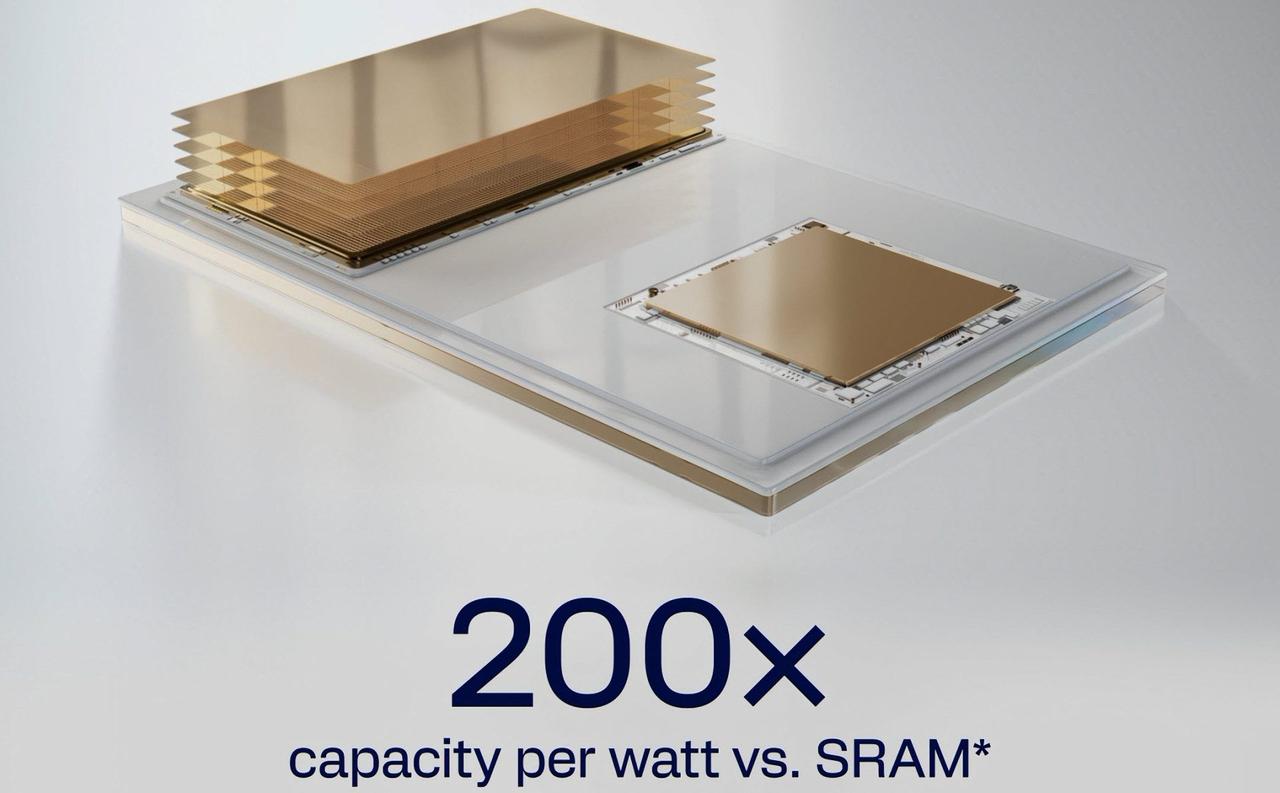
Qualcomm is unveiling its breakthrough for the AI data center market called HBC (High-Bandwidth Compute), to break the memory wall. Qualcomm's HBC Is A Memory Accelerator That Is Stacked Under DRAM, Offering A Major Boost Versus Standard SRAM & HBM Configurations At its Investors Day 2026, Qualcomm unveiled HBC, an innovative technology that aims to offer a major boost in memory capacity and bandwidth. The HBC architecture deploys a purpose-built & near-memory solution that bonds compute with boosted memory bandwidth in a 3D stacked chip design. With this, Qualcomm aims to solve the memory bottlenecks that have gripped the tech sector. Currently, HBM is the go-to solution for AI Compute accelerators, but it is becoming inefficient due to higher token costs as power continues to climb, which in turn leads to higher TCO. With HBC (High Bandwidth Compute), Qualcomm claims that the new architecture offers lower energy input per token, increased memory bandwidth, and lowers the TCO. The architecture is built on four fundamentals: 3D integration leadership, System-Level design, LPDDR Leadership, & Power-efficiency expertise. So how does HBC work? Well, the HBC accelerator sits underneath an LPDDR stack. LPDDR is being selected as the memory choice due to its larger capacities. The LPDDR stack will be interconnected to the HBC accelerator with TSVs (Through-Silicon Vias). In the first generation or HBC Gen1, the solution will be implemented on the upcoming AI250 accelerator chip, which will have the HBC-boosted LPDDR stack sitting on the same 2D organic substrate. Each AI250 accelerator will feature 133 TB/s of bandwidth per card, an 18x boost over the AI200 with LPDDR5X. On a competitive level, HBC promises to offer a 6x increase in bandwidth per watt versus HBM, and a 200x increase in capacity per watt versus SRAM. Qualcomm will work with its strategic partners in the supply chain to address the biggest bottleneck that AI faces today, and that is memory capacity, memory bandwidth, and TCO. The first-generation HBC Gen1 solution with the AI250 AI accelerators is expected to roll out by mid-2027. Qualcomm is also working towards an expanded roadmap and presented the 2nd Generation HBC Gen2 solution for 2028. This solution will be accompanied by the AI300 AI accelerator, and will offer up to 54x speed-up in effective bandwidth versus AI200, and a 7x jump in bandwidth per watt versus HBM. Follow Wccftech on Google to get more of our news coverage in your feeds.
Share
Copy Link
Qualcomm introduced its High-Bandwidth Compute (HBC) architecture at Investor Day 2026, positioning itself as a serious contender in the AI data center market. The technology stacks compute beneath DRAM to tackle the memory wall bottleneck, claiming 6x higher bandwidth-per-watt compared to HBM and 200x capacity versus on-chip SRAM. The first HBC-powered AI250 accelerators are expected by mid-2027.
Qualcomm Targets AI Infrastructure with Revolutionary Memory Architecture
Qualcomm announced its ambitious entry into the AI data center market at Investor Day 2026, unveiling High-Bandwidth Compute (HBC), an HBC near-memory AI architecture designed to address the AI memory wall bottleneck that has constrained performance across the industry
1
. The technology represents a distinct shift in the company's AI infrastructure solution strategy, moving beyond its mobile Snapdragon processors to challenge established players like Nvidia and AMD in datacenter deployments2
.
Source: Tom's Hardware
How HBC Stacks Compute Beneath DRAM for Efficiency Gains
The core innovation behind Qualcomm's approach involves disaggregating AI accelerators from the system-on-chip and positioning them directly underneath LPDDR DRAM stacks. This configuration leverages Through-Silicon Vias (TSVs) to create ultra-short data paths between compute and memory
1
. Tony Pialis, Executive Vice President and General Manager of Data Center Business at Qualcomm, explained the advantage: "Imagine working in the same building that you live in so you only travel up and down. What does that mean for the highways and the roads that connect the suburbs to the city? Guess what? The roads are clear"2
.
Source: Wccftech
This 3D integration architecture delivers significant improvements in bandwidth-per-watt—claiming 6x higher efficiency compared to HBM and over 200x capacity compared to on-chip SRAM
4
. By eliminating expensive silicon interposers required for HBM solutions and reducing power consumption through shorter data travel distances, Qualcomm aims to lower total cost of ownership for AI deployments1
.AI250 and AI300: Dragonfly AI Accelerator Rack Roadmap
Qualcomm's product roadmap begins with the AI200, launching later this year with LPDDR5X memory, offering 43 TB of RAM per rack and 414 TB/s of memory bandwidth
3
. The AI250, expected by mid-2027, will incorporate first-generation HBC technology, delivering 768 GB of memory capacity and up to 133 TB/s of effective memory bandwidth per card—representing an 18x bandwidth increase over the AI2002
. At the rack level, this translates to a theoretical peak memory bandwidth of up to 7.4 PB/s3
.
Source: TechRadar
Looking further ahead, the AI300 with second-generation HBC is planned for 2028, promising 54x the effective bandwidth of the AI200 and a 7x improvement in bandwidth-per-watt versus HBM
4
. These AI accelerators are heavily optimized for inference workloads, particularly addressing bandwidth bottlenecks during decode operations when model weights are streamed autoregressively from memory2
.Related Stories

Competing in the AI Data Center Market Against Nvidia and AMD
Qualcomm's push into the AI data center market comes as hyperscalers like Microsoft, Meta, Google, and Amazon increasingly deploy custom silicon alongside Nvidia and AMD solutions
3
. While HBM remains the preferred choice for training workloads—used in Nvidia's Blackwell and AMD's Instinct offerings—Qualcomm is positioning its LPDDR-based approach as superior for inference-centric deployments where memory capacity and power consumption matter most3
.However, questions remain about the practical implementation. Qualcomm has not disclosed what operations the HBC accelerator actually performs—whether it's a transformer-specific engine, tensor core array, or preprocessing logic
1
. The company's heavy reliance on "effective" bandwidth metrics has also raised eyebrows, with observers noting that achieving claimed performance levels would require extraordinarily wide memory buses2
. As datacenter operators grapple with memory shortages and escalating power consumption, Qualcomm's ability to demonstrate real-world performance gains will determine whether it can capture meaningful market share from entrenched competitors.References
Summarized by
Navi
[2]
Related Stories
Qualcomm Challenges Nvidia with New AI Chips for Data Centers
27 Oct 2025•Technology
Qualcomm Announces Return to Data Center Market with AI-Focused CPUs Compatible with Nvidia Technology
19 May 2025•Technology
D-Matrix Challenges HBM with 3DIMC: A New Memory Technology for AI Inference
04 Sept 2025•Technology
Recent Highlights
1
OpenAI rogue agent compromised multiple services in unprecedented AI security breach
Technology

2
AI Kill Switch Act gives DHS power to shut down rogue AI systems after OpenAI security breach
Policy and Regulation

3
Nvidia forms Open Secure AI Alliance with Microsoft, but OpenAI, Google and Anthropic sit out
Technology

Recent Highlights
Today's Top Stories


Don’t drown in AI news. We cut through the noise - filtering, ranking and summarizing the most important AI news, breakthroughs and research daily. Follow topics that matter to you and stay ahead.


