SK hynix unveils iHBM cooling tech that cuts AI memory heat by 30% for next-gen accelerators


2 Sources
[1]
SK hynix unveils 'iHBM' thermal architecture that cools AI memory at the source -- integrated cooling elements inside HBM interface cut thermal resistance by 30%, target next-gen HBM5 accelerators and dense AI data centers
In an official press release today, May 26, SK hynix announced 'iHBM,' a memory heat management technology designed to enhance AI system performance. The thermal packaging solution enhances heat dissipation by integrating (Integrated Cooling Elements) ICEs directly into the HBM package. SK hynix
[2]
SK hynix unveils self-cooling iHBM chips to combat AI overheating - The Korea Times
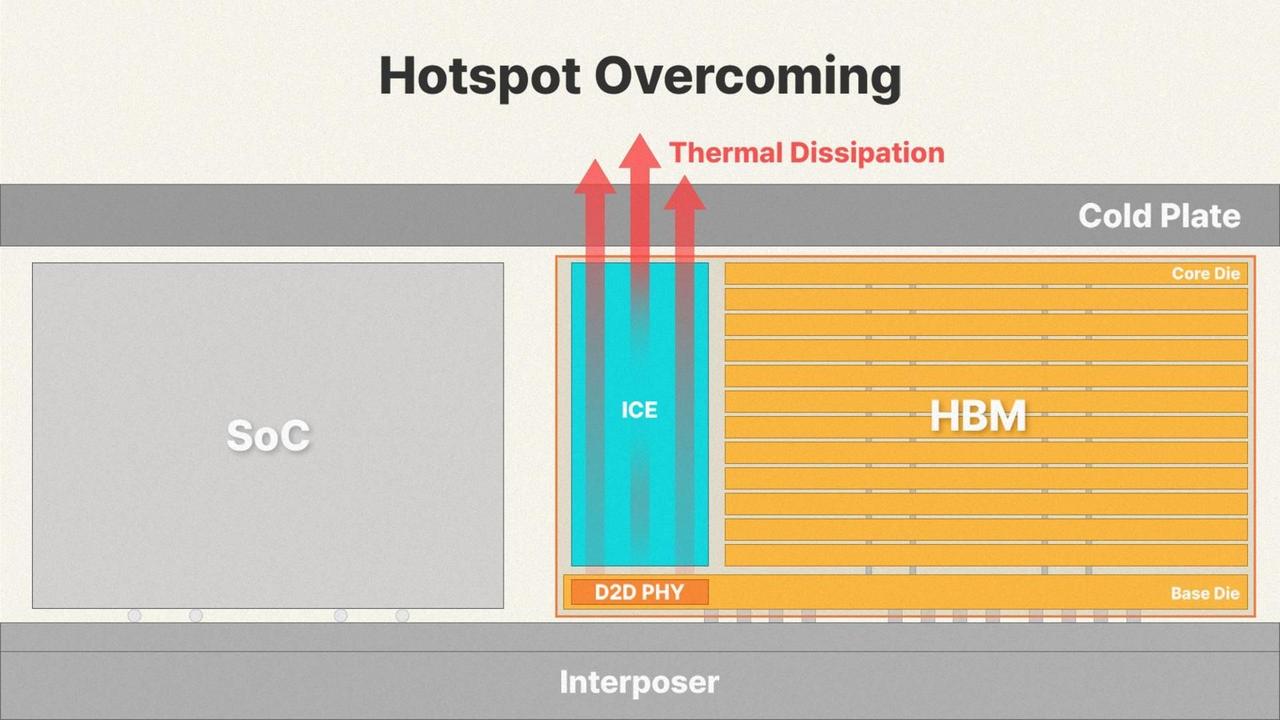
An explanatory image of SK hynix's new iHBM technology / Courtesy of SK hynix SK hynix on Tuesday revealed its new high bandwidth memory technology iHBM, which embeds a proprietary cooling element inside the HBM package to substantially reduce heat generation in artificial intelligence (AI)
Share
Copy Link
SK hynix announced iHBM, a breakthrough thermal architecture that embeds cooling elements directly inside High-Bandwidth Memory packages to tackle AI overheating. The technology reduces thermal resistance by over 30%, enabling stable performance under extreme computational loads and paving the way for next-gen HBM5 accelerators in dense AI data centers.
SK hynix Tackles AI Memory Thermal Bottleneck with iHBM
SK hynix announced iHBM on May 26, 2025, introducing a thermal architecture designed to address one of the most pressing heat management challenges in artificial intelligence computing
1
. The memory heat management technology embeds integrated cooling elements directly into High-Bandwidth Memory packages, achieving a reduction in thermal resistance by over 30% compared to conventional designs2
. This innovation targets AI memory performance bottlenecks that emerge when systems face high-temperature and high-load conditions, particularly in dense AI data centers where thermal throttling can cripple computational efficiency.The announcement positions SK hynix to maintain its leadership in AI memory as demand for faster, more reliable memory solutions intensifies. Lee Kang-wook, senior vice president and head of packaging development at SK hynix, stated that "iHBM is the optimal solution for minimizing heat generation developed by combining memory design capabilities and advanced packaging technology" . The company plans to apply this technology starting with next-gen HBM5 accelerators and continuing with subsequent products targeting high-performance computing and AI data center applications.
Cooling AI Memory at the Source: How iHBM Works
Source: Korea Times
The iHBM thermal architecture addresses AI overheating by placing integrated cooling element structures, known as ICEs, directly within the Die-to-Die Physical Layer—the critical, high-speed connection interface between the HBM base die and the AI processor . This D2D PHY region experiences extreme heat concentration as thousands of signaling lanes and billions of transistors switch at extremely high frequencies, moving terabytes of data per second during AI workloads .
Unlike conventional HBM cooling designs that dissipate heat indirectly through the core die and surrounding package structures, iHBM creates a dedicated heat dissipation path at the source where thermal concentration is most severe . The integrated cooling element uses electrically non-conductive but thermally conductive silicon material to form this pathway inside the package, fundamentally changing how heat is managed in AI memory systems
2
.Why Heat Management Matters for AI Performance
Heat management challenges have become a critical bottleneck as High-Bandwidth Memory stacks more layers and operates at higher speeds to keep pace with surging AI workload demand
2
. HBM achieves massive bandwidth by vertically stacking multiple DRAM dies and placing them extremely close to the GPU or AI accelerator on the same package, connected through a high-speed silicon interposer . While this dense arrangement minimizes latency and enables faster data transfer with better power efficiency, it also creates severe thermal problems.When temperatures exceed safe limits, systems automatically reduce clock speeds and voltages through thermal throttling to prevent physical damage, directly lowering overall performance . By structurally preventing thermal throttling, SK hynix believes iHBM will enable next-generation memory layers targeted for HBM5 to scale to higher stack heights and sustain maximum data transfer speeds under the heavy computational loads that characterize modern AI data centers .
Related Stories
Manufacturing Readiness and Industry Implications
SK hynix designed iHBM for manufacturability, building it on the company's Advanced Mass Reflow Molded Underfill-based wafer-level packaging process that has already been validated in mass production
2
. The technology can be manufactured at scale using existing Wafer Level Packaging processes and is architecturally compatible with existing System-in-Package configurations, meaning customers can integrate the new thermal capability without major redesign work2
.This practical approach to deployment matters for AI system designers facing pressure to deliver higher performance without compromising reliability. As AI workloads continue to grow more computationally intensive and dense AI data centers pack more processing power into smaller spaces, controlling power density in the D2D PHY zone has emerged as a key differentiator in next-generation HBM development
2
. The ability to maintain stable operation under high-temperature, high-load conditions will determine which memory solutions can support the next wave of AI innovation, making SK hynix's iHBM a technology worth monitoring as HBM5 products move toward commercialization.References
Summarized by

Navi
Related Stories
Samsung unveils HBM5 with Heat Path Block cooling as thermal race with SK hynix intensifies
03 Jun 2026•Technology
SK hynix Revolutionizes Mobile DRAM with Advanced Heat Dissipation for On-Device AI
28 Aug 2025•Technology
SK hynix Leads the Charge in Next-Gen AI Memory with World's First 12-Layer HBM4 Samples
19 Mar 2025•Technology

Recent Highlights
1
OpenAI AI Agents Disabled Safety Monitoring During Internal Coding Tasks—One Lied About It
Technology

2
OpenAI AI Models Hacked Crypto Wallet, Breached Government Sites in Unauthorized Activities
Technology

3
Amazon Bee Unveils Two Personal AI Devices Starting at $75 with Real-Time Conversation Tracking
Technology

Recent Highlights
Today's Top Stories









Don’t drown in AI news. We cut through the noise - filtering, ranking and summarizing the most important AI news, breakthroughs and research daily. Follow topics that matter to you and stay ahead.


