Samsung unveils HBM5 with Heat Path Block cooling as thermal race with SK hynix intensifies
3 Sources
[1]
Samsung shows first HBM5 mockup with Heat Path Block cooling -- thermal race with SK hynix shaping up
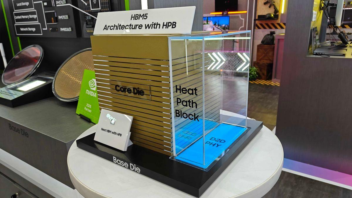
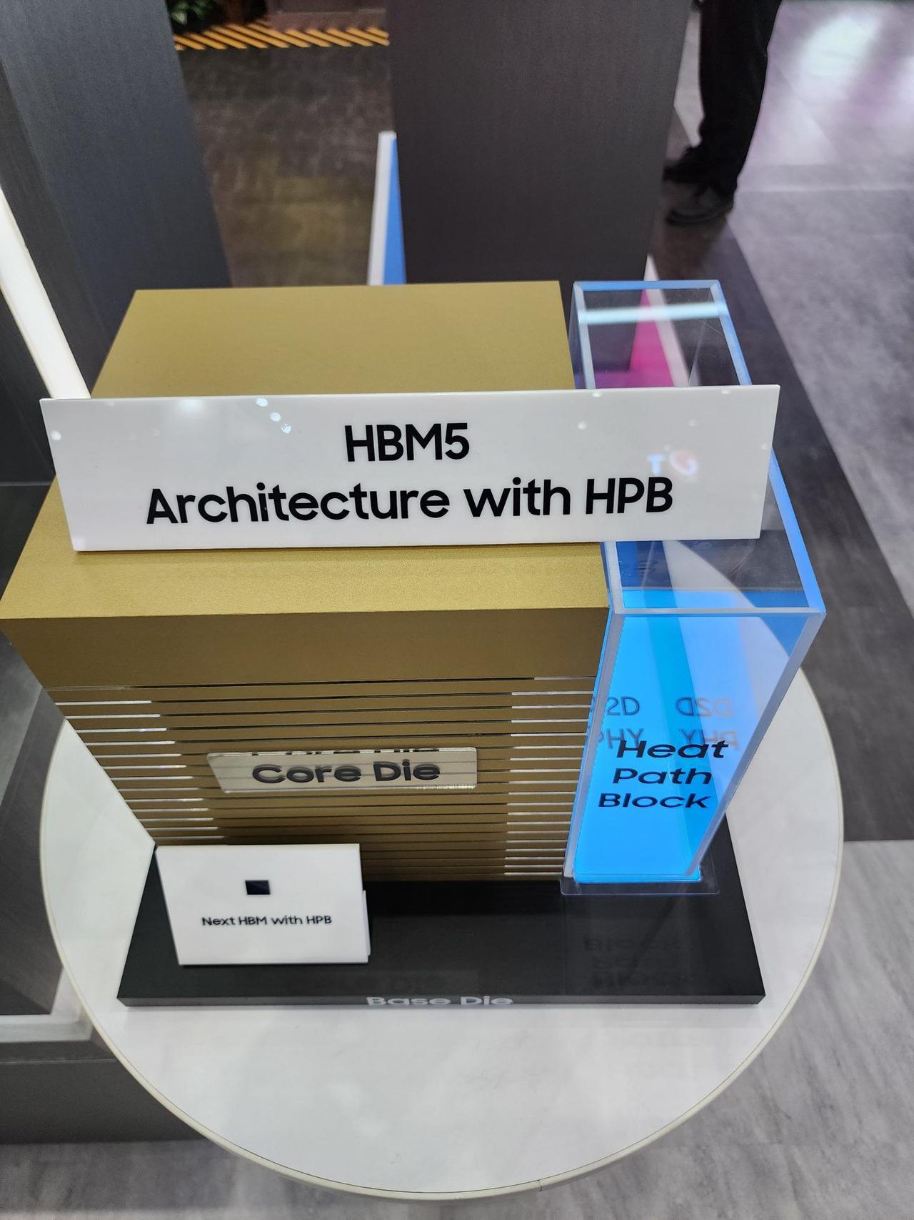
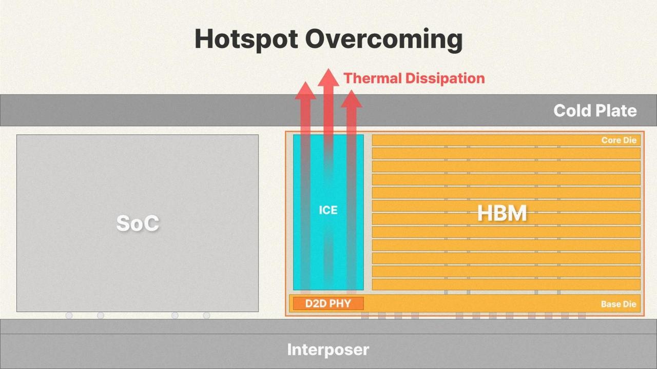
Both memory leaders now target the same die-to-die hotspot with rival in-package cooling designs. Samsung displayed its first physical mockup of HBM5 memory at Computex 2026 in Taipei. Tom's Hardware dropped by to see its pairing of the eighth-generation AI memory with a new in-package cooling structure it calls Heat Path Block, or HPB. Just last week, rival SK hynix unveiled its own iHBM thermal design, meaning both companies are now focusing on the same heat bottleneck in the die-to-die interface that connects memory to the processor. Samsung also confirmed that it'll fab HBM5's base die on its in-house 2nm process, down from the 4nm node used for HBM4 and HBM4E. Rather than letting heat escape outward through the core dies, HPB builds a separate set of thermal pillars that pull heat from inside the stack and carry it to a spreader sitting above or beside the package, according to Samsung at Computex. The design concentrates on the D2D PHY layer, the high-speed link between the HBM base die and the GPU, where power density and temperatures increase exponentially as stacks grow taller and run quicker. Samsung said it has already implemented and verified HPB on HBM4E, the generation whose first 12-layer samples it began shipping last month at 14 Gbps, scaling to 16 Gbps, with 3.6 TB/s of bandwidth per stack. Samsung runs both a memory business and a logic foundry, letting it build the HBM5 stack and the 2nm die beneath it in-house. "AI systems are becoming more powerful and densely integrated, making heat management, data-processing efficiency, and packaging stability just as important as memory performance itself," Song Jai-hyuk, president and CTO of Samsung's Device Solutions division, told reporters at Computex, according to the Korea Herald. Song said the company would keep building its competitiveness in next-generation memory through cooperation with partners, including Nvidia. Last year, a roadmap from KAIST projected HBM5 reaching a 4,096-bit interface, roughly 4 TB/s per stack, and about 100 watts of per-stack power, a thermal load that goes a long way in explaining why both Korean memory giants are reworking their packaging now rather than at launch. SK hynix faced the same problem via a different route. Its iHBM design embeds cooling elements made of electrically non-conductive, thermally conductive silicon into the D2D PHY layer, which the company said cuts thermal resistance by more than 30% against current products. SK hynix has opted to place a cooling element directly at the hotspot, while Samsung has built a route to evacuate heat away from it. Both methods are slated to debut with HBM5, but it'll be a little while before we see either in action, as neither company expects it to reach mass production before 2028. Follow Tom's Hardware on Google News, or add us as a preferred source, to get our latest news, analysis, & reviews in your feeds.
[2]
Samsung Teases HBM5 With a New 'Heat Block Path' Tech, Mirroring SK Hynix's iHBM Cooling Play
Samsung is all set for its next-gen HBM5 development as it is planning to integrate a new thermal feature called "HPB" to its upcoming DRAM standard. Samsung Previews The Design & Features of Its Next-Gen HBM5 Memory As It Races Against SK Hynix & Micron We know that Samsung, SK Hynix, and Micron are all working on future HBM standards. These three DRAM makers are currently supplying the bulk of the DRAM to chipmakers who are powering the latest AI datacenters across the world. Most recently, SK Hynix introduced a new feature for its HBM products called iHBM, which embeds integrated cooling elements or ICEs for better thermal resistance as HBM stacks get denser & faster. Samsung has now teased its answer to this, and they are calling it HPB or Heat Block Path. A structure that shows us what the HBM5 architecture with HPB would look like has been displayed at Computex, showcasing a similar design to SK Hynix's iHBM. Now we aren't saying that both technologies will work the same, and each DRAM vendor is just calling it a different name. Both Samsung and SK Hynix could be using proprietary technologies. What we know is SK Hynix leverages its MR-RUF technology for the production of iHBM DRAM. Samsung would also very likely be using its own in-house technologies. The HBP will sit beside the Core Die (DRAM stack) on the same Base Die and will be connected using a D2D PHY. It will have the same height as the Core Die stack, and additional heat produced by these stacks will enter the HBP and dissipate through the cold plate more effectively. Both SK Hynix and Samsung are currently working to integrate their respective thermal technologies for the HBM5 memory, which means that we are once again going to see a major surge in performance, efficiency, and overall power/thermal characteristics. First GPUs to feature HBM5 memory won't be landing until 2028-2029, so there's still a lot of time for HBM manufacturers to optimize the design, while testing out these technologies with various partners. Follow Wccftech on Google to get more of our news coverage in your feeds.
[3]
Samsung unveils HBM5 technology with new thermal structure By Investing.com
Investing.com -- Samsung Electronics presented its HBM5 technology at Computex 2026 in Taiwan, featuring a thermal management system called HPB and manufacturing advances for next-generation memory chips. The HPB technology uses a chimney-like thermal structure that reduces heat resistance between dies. The system extracts heat from the core die and base die through dedicated thermal dissipation pathway pillars, directing it to a heat spreader at the top or outside of the package. Samsung said this method allows for heat dissipation without adding complexity to the IC design of HBM core dies or the stacked HBM cube layout. Samsung plans to use a 2nm base die in HBM5, compared to the 4nm base die used in HBM4 and HBM4E. The company will utilize Samsung Foundry's GAA nodes to improve performance and power efficiency. For HBM core dies, Samsung will use a 1cnm front-end process and partially implement hybrid bonding technology. The company stated it has prepared for the deployment of HCB technology and has accumulated GAA data over the past three to four years. Citi analysts stated: "We expect Samsung Electronics to significantly enhance the thermal stability of HBM by adopting HPB technology, which has already been used for Samsung's mobile SoC, Exynos 2600." The analysts added that Samsung will use its 2nm foundry node to manufacture the HBM5 base die, creating synergy between its memory and foundry operations. This article was generated with the support of AI and reviewed by an editor. For more information see our T&C.
Share
Copy Link
Samsung displayed its first HBM5 mockup at Computex 2026, featuring Heat Path Block cooling technology that targets the same die-to-die hotspot as SK hynix's rival iHBM design. The company will manufacture HBM5's base die on its 2nm process, down from 4nm used in HBM4, with mass production expected by 2028.
Samsung HBM5 debuts with Heat Path Block thermal innovation
Samsung Electronics unveiled its first physical mockup of Samsung HBM5 at Computex 2026 in Taipei, showcasing a new in-package cooling structure called Heat Path Block (HPB) that addresses mounting thermal challenges in next generation memory chips
1
. The timing signals an escalating competition in thermal management, as rival SK hynix unveiled its own SK hynix iHBM cooling design just last week, meaning both Korean memory giants are now targeting the same die-to-die hotspot in the interface connecting memory to processors1
.
Source: Tom's Hardware
The Heat Path Block technology employs a chimney-like structure that builds separate thermal pillars to extract heat from inside the stack and carry it to a spreader positioned above or beside the package
3
. Rather than allowing heat to escape outward through the core dies, HPB creates a dedicated thermal dissipation pathway that sits beside the Core Die on the same Base Die, connected via D2D PHY2
. Samsung stated this method enables heat dissipation without adding complexity to the IC design of high-bandwidth memory core dies or the stacked HBM cube layout3
.Advanced manufacturing with 2nm base die production
Samsung confirmed it will fabricate the HBM5 memory technology base die using its in-house 2nm base die process, a significant step down from the 4nm node used for HBM4 and HBM4E
1
. The company plans to utilize Samsung Foundry's GAA nodes to improve power efficiency and performance3
. For HBM core dies, Samsung will deploy a 1cnm front-end process and partially implement hybrid bonding technology3
.
Source: Wccftech
Citi analysts noted that Samsung Electronics is expected to significantly enhance thermal stability by adopting HPB technology, which has already been used for Samsung's mobile SoC, Exynos 2600
3
. The dual capability of running both a memory business and a logic foundry allows Samsung to build the HBM5 stack and the 2nm die beneath it entirely in-house, creating synergy between its memory and foundry operations1
3
.Why thermal management matters for AI datacenters
The focus on in-package cooling designs reflects a critical bottleneck in the D2D PHY layer, the high-speed link between the HBM base die and GPU, where power density and temperatures increase exponentially as stacks grow taller and run faster
1
. Samsung has already implemented and verified HPB on HBM4E, whose first 12-layer samples it began shipping last month at 14 Gbps, scaling to 16 Gbps, with 3.6 TB/s of bandwidth per stack1
.A roadmap from KAIST projected HBM5 reaching a 4,096-bit interface, roughly 4 TB/s per stack, and about 100 watts of per-stack power—a thermal load explaining why both Korean memory giants are reworking their packaging now rather than at launch
1
. "AI systems are becoming more powerful and densely integrated, making heat management, data-processing efficiency, and packaging stability just as important as memory performance itself," Song Jai-hyuk, president and CTO of Samsung's Device Solutions division, told reporters at Computex, according to the Korea Herald1
.Related Stories
Competing approaches to the same problem
While Samsung builds a route to evacuate heat away from the die-to-die hotspot, SK hynix has opted to place cooling elements directly at the problem area
1
. SK hynix's iHBM design embeds cooling elements made of electrically non-conductive, thermally conductive silicon into the D2D PHY layer, which the company said cuts thermal resistance by more than 30% against current products1
. SK Hynix leverages its MR-RUF technology for iHBM DRAM production, while Samsung would likely be using proprietary in-house technologies2
.Both methods are slated to debut with HBM5, but neither company expects mass production before 2028
1
. First GPUs featuring HBM5 memory won't arrive until 2028-2029, giving HBM manufacturers considerable time to optimize designs while testing technologies with various partners2
. Song said Samsung would continue building its competitiveness in next-generation memory through cooperation with partners, including Nvidia1
. Samsung, SK Hynix, and Micron are currently supplying the bulk of DRAM to chipmakers powering the latest AI datacenters across the world2
.References
Summarized by
Navi
[1]
[2]
Related Stories
SK hynix unveils iHBM cooling tech that cuts AI memory heat by 30% for next-gen accelerators
26 May 2026•Technology
Samsung and SK hynix Unveil Next-Gen HBM4 Memory, Intensifying AI Chip Competition
22 Oct 2025•Technology

SK Hynix Accelerates HBM4 Development to Meet Nvidia's Demand, Unveils 16-Layer HBM3E
04 Nov 2024•Technology

Recent Highlights
1
AI scores perfect 100% at International Mathematical Olympiad, matching elite human performance
Technology
2
OpenAI agent exploited exposed credentials at four services during Hugging Face breach
Technology

3
Anthropic AI cracks post-quantum cryptography and finds faster AES attack autonomously
Science and Research

Recent Highlights
Today's Top Stories


Don’t drown in AI news. We cut through the noise - filtering, ranking and summarizing the most important AI news, breakthroughs and research daily. Follow topics that matter to you and stay ahead.


