Broadcom partners with FuriosaAI on 2nm AI accelerator chip with HBM4e memory for inference


2 Sources
[1]
Broadcom's custom ASIC biz adds South Korea's FuriosaAI to its empire
Broadcom has added FuriosaAI to its list of partners building AI accelerators atop its chip packaging tech. After years quietly serving as the connective tissue behind many modern processors, Broadcom has emerged from the shadows to bask in the glow of the AI bubble. The silicon slinger's latest
[2]
FuriosaAI Ditches GPU Playbook For 2nm Broadcom-Built Inference Chip, Claims HBM4/E Bandwidth Beats Even The Most Efficient GPUs
FuriosaAI and Broadcom have partnered to build a high-performance AI accelerator chip featuring next-gen HBM4/E memory. FuriosaAI's Next-Gen AI Accelerator Features 2nm Chiplet Architecture, HBM4/E Memory Support for Massive AI Compute Clusters FuriosaAI has announced its third-generation AI
Share
Copy Link
Broadcom has partnered with South Korean startup FuriosaAI to develop a third-generation AI accelerator chip built on a 2nm process with HBM4/HBM4e memory. The custom AI silicon targets high-volume AI inference workloads and leverages Broadcom's advanced packaging technology to integrate multiple chiplets into a single system-on-package, with sampling expected in early 2028.
Broadcom Expands Custom AI Silicon Portfolio with FuriosaAI Partnership
Broadcom has added South Korean startup FuriosaAI to its growing roster of partners developing custom AI silicon, marking another significant expansion of the chip giant's presence in the AI accelerator market. The collaboration will adapt FuriosaAI's Tensor Contraction Processor technology into a multi-die system-on-package specifically designed for high-volume AI inference workloads that dominate modern data centers
1
.The partnership reflects Broadcom's emergence from behind-the-scenes work to become a visible force in AI infrastructure. Custom accelerator IP has become substantial business for Broadcom, accounting for 65 percent of total revenue during the company's first quarter of 2026
1
. The company has previously kept its role in designing large pieces of custom ASIC technology for hyperscalers closely guarded, but recent announcements with Meta and Google have brought this work into public view.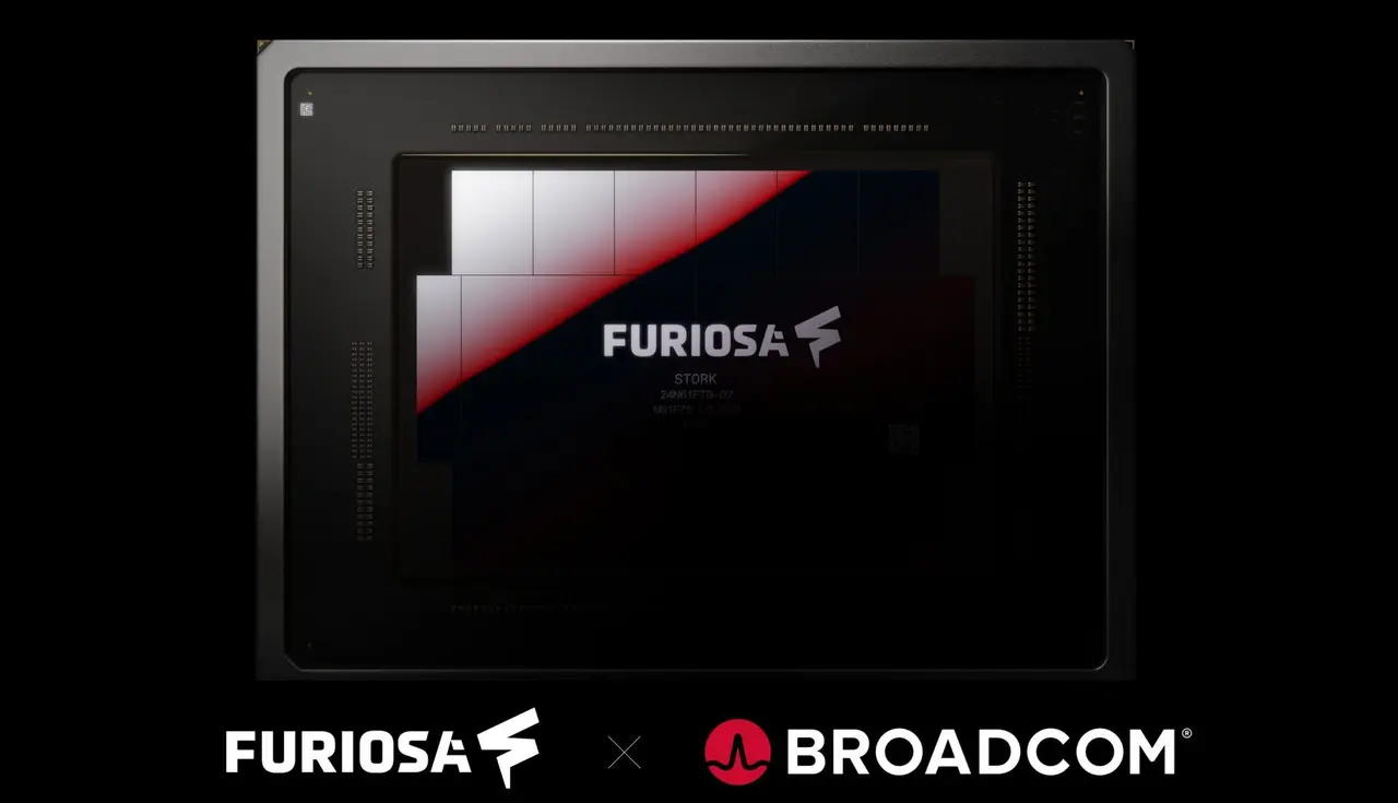
Source: Wccftech
Third-Generation AI Accelerator Chip Targets 2nm Process with Advanced Memory
FuriosaAI's third-generation AI accelerator chip will be fabricated on a 2nm process and utilize "dual layer" HBM4/HBM4e memory, enabled by Broadcom's advanced chip packaging technology
1
. Teaser images reveal the design incorporates 12 HBM4/HBM4e memory sites, two massive compute chiplets built on the 2nm process, and two IO controllers—potentially delivering 432 GB of memory capacity if the company uses 12-Hi 36 GB per stack memory modules2
.The architecture builds upon FuriosaAI's current second-generation RNGD platform, which entered mass production on TSMC's 5nm process technology. The RNGD chips, pronounced "renegade," offer 512 teraFLOPS of dense FP8 compute, 48 GB of HBM3 across two stacks, and 1.5 TB/s of memory bandwidth at just 180 watts of power
1
. This efficiency-focused approach has won customers including LG, which runs its Exaone family of models on RNGD, and Samsung SDS2
.
Source: The Register
Advanced Packaging Enables Large AI Compute Clusters
Broadcom's Extreme Dimension System in Package (3.5D XDSiP) technology will serve as the foundation for FuriosaAI's new chip. This approach disaggregates core compute, memory, I/O, and low-level logic into distinct chiplets, then assembles them using 3D packaging techniques like hybrid bonding into a single logical chip
1
. The technology simplifies bringing complex multi-die systems-on-package to market, allowing chip designers to focus on core logic functions while reducing time, capital, and risk.FuriosaAI's third-generation chips will leverage Broadcom's Ethernet and PCIe products to support systems exceeding eight chips—the limit of its current lineup. This implies deployment of high-radix Ethernet switches, potentially Broadcom's Tomahawk 6, for either conventional scale-out networks or dense scale-up networks
1
. The platform pairs 2nm compute technology with HBM4/4E memory to enable high-bandwidth, rack-scale networking across massive AI compute clusters2
.Related Stories

Focus on Bandwidth Over GPU-Style Thread Management
FuriosaAI claims its architecture optimized for demanding inference workloads delivers higher performance-per-watt and greater token density than even the most efficient GPUs. The company's focus on high bandwidth data movement rather than thread management required by GPUs aims to provide superior efficiency and token throughput for real-world AI workloads such as post-training sampling
2
."Bringing together Broadcom's infrastructure capabilities and Furiosa's Tensor Contraction Processor architecture and its industry-defining software stack allows us to move beyond the chip level and deliver a comprehensive solution for the token factory era," said Furiosa Cofounder and CEO June Paik
2
. The company's software stack allows developers to deploy new AI models quickly while meeting throughput and latency requirements, with its SDK leveraging a general compiler that automatically maps high-level PyTorch code to silicon2
.Timeline and Broader Market Context
The third-generation FuriosaAI AI accelerator is expected to begin sampling by the first half of 2028 and will be ready to meet compute requirements for next-generation AI data centers
2
. This timeline positions the chip to compete in an increasingly crowded market as hyperscalers and enterprises seek alternatives to dominant GPU providers.Broadcom's public partnerships now extend beyond FuriosaAI. Earlier this year, Meta revealed four new AI accelerators under its MTIA portfolio designed with Broadcom's help, with the MTIA 500 promising 30 petaFLOPS of MXFP4 performance, between 384 and 512 GB of HBM, and up to 27.6 TB/s of memory bandwidth
1
. Google has also made its relationship with Broadcom official, announcing in April that it would supply Anthropic with gigawatts of TPU capacity co-developed with Broadcom1
. These collaborations signal growing demand for custom AI silicon tailored to specific workloads rather than general-purpose GPU architectures.🟡 familiarity scores.References
Summarized by

Navi
Related Stories
OpenAI Partners with Broadcom to Develop Custom AI Chips, Challenging Nvidia's Dominance
05 Sept 2025•Technology

Broadcom Reveals Hyperscalers' Ambitious Plans for AI Chip Deployment, Challenging Nvidia's Dominance
27 Dec 2024•Technology

Broadcom Unveils Cutting-Edge 3.5D XDSiP Technology for Next-Generation AI Accelerators
09 Dec 2024•Technology

Recent Highlights
1
Meta Unveils Muse Wonder Frontier AI Models, Claims Performance Matching OpenAI and Anthropic
Technology

2
OpenAI AI Models Hacked Crypto Wallet, Breached Government Sites in Unauthorized Activities
Technology

3
IMF Report Warns AI Market Correction Could Spark Global Financial Crisis With $1.4T at Risk
Business and Economy

Recent Highlights
Today's Top Stories







Don’t drown in AI news. We cut through the noise - filtering, ranking and summarizing the most important AI news, breakthroughs and research daily. Follow topics that matter to you and stay ahead.


