7 Sources
[1]
US to award GlobalFoundries $300 million to develop faster AI chip links
July 29 (Reuters) - GlobalFoundries (GFS.O), opens new tab said on Wednesday the U.S. government will award $300 million to the chipmaker to bolster research and development of silicon photonics technology to power more efficient AI data centers. The award is part of President Donald Trump's effort to direct CHIPS Act research funding toward critical semiconductor technologies as Washington seeks to strengthen its position in the global race with China. The administration has previously committed $150 million for semiconductor manufacturing â equipment and $2 billion for quantum computing. Silicon photonics uses light instead of electrical signals to move data between chips, enabling higher bandwidth and lower power consumption for AI systems. The funding from the U.S. Department of Commerce is also aimed at advancing co-packaged optics (CPO), a technology that integrates silicon photonics directly alongside AI processors to further boost data-transfer speeds and energy efficiency. Much of the supply chain for silicon â photonics and advanced optical packaging is currently concentrated outside the United States, with major manufacturers including Taiwan's TSMC (2330.TW), opens new tab and Israel's Tower Semiconductor (TSEM.TA), opens new tab. GlobalFoundries said it is targeting to boost data transfer speeds to 400 gigabits per second â and up to five times greater energy efficiency than current-generation implementations. "GlobalFoundries has spent more than a decade building the technology, footprint and ecosystem to â lead this transition, and we have the proven manufacturing foundation to scale it -- in the United States," said Tim Breen, CEO â of GlobalFoundries. The research will use the company's facilities in Malta, New York, and Burlington, Vermont. Reporting by Harshita Mary Varghese in Bengaluru and Stephen Nellis in San Francisco; Editing by Vijay Kishore Our Standards: The Thomson Reuters Trust Principles., opens new tab
[2]
GlobalFoundries wins $300 million CHIPS Act silicon photonics award
The semiconductor maker will use the funds to develop optical chip interconnect technologies aimed at boosting AI data center performance GlobalFoundries announced Wednesday that it has signed a letter of intent with the U.S. Department of Commerce for a $300 million CHIPS Act award to advance silicon photonics research and development. Silicon photonics transmits data via light rather than electricity, which allows AI systems to achieve greater bandwidth while drawing less power. Among the technologies the funding will support is co-packaged optics, an approach that places silicon photonics circuitry in direct proximity to processors, along with next-generation optical materials, wafer technologies, and advanced packaging, all with the goal of improving interconnect performance and reducing energy use. GlobalFoundries said its goals include reaching 400 gigabits per second in data transfer throughput and cutting energy consumption to a fifth of what current-generation systems require. GlobalFoundries plans to conduct the work at its campuses in Malta, New York, and Burlington, Vermont. As part of a separate agreement tied to the award, the U.S. Department of Commerce will receive an equity stake in GlobalFoundries representing approximately 1% ownership, the company said. "Silicon photonics is essential to AI infrastructure," GlobalFoundries CEO Tim Breen said in a statement. "GlobalFoundries has spent more than a decade building the technology, footprint and ecosystem to lead this transition, and we have the proven manufacturing foundation to scale it -- in the United States." Much of the supply chain for silicon photonics and advanced optical packaging is currently concentrated outside the United States, according to Reuters. Commerce Secretary Howard Lutnick said in a statement that the investment would "enhance our country's domestic capabilities, create high-paying jobs and keep America at the forefront of the semiconductor industry." The announcement drew support from several major technology companies. NVIDIA founder and CEO Jensen Huang said in a statement that silicon photonics is "essential" to scaling U.S. manufacturing. Executives from AMD $AMD, Broadcom $AVGO, Cisco $CSCO, Meta $META, Microsoft $MSFT, and Qualcomm $QCOM also issued statements endorsing the investment. The CHIPS Act award is part of the Trump administration's broader effort to direct research funding toward critical semiconductor technologies. The administration has previously committed $150 million for semiconductor manufacturing equipment and $2 billion for quantum computing, according to Reuters.
[3]
GlobalFoundries to receive $300M in federal funding for silicon photonics research
The U.S. government will provide GlobalFoundries with $300 million in funding to support its silicon photonics research. The U.S. Commerce Department committed to providing the capital in a letter of intent that was announced today. As part of the transaction, the government will take a 1% stake in GlobalFoundries. The development comes two months after the chipmaker secured a separate $375 million federal grant for a new quantum chip foundry. GlobalFoundries operates fabs that produce chips based on customer-provided designs. One of the company's specialties is making low-power processors that don't require the latest manufacturing technologies. Additionally, GlobalFoundries produces auxiliary chips optimized for tasks filtering Wi-Fi inference. Silicon photonics, the focus of the company's agreement with the Commerce Department, is an umbrella term for the chips that power fiber-optic networks. Such networks power many of the world's artificial intelligence data centers. GlobalFoundries will use the federal funding to accelerate its silicon photonics research and development efforts. The initiative will place particular emphasis on a technology known as co-packaged optics, or CPO. Server switches represent the data traffic they process as electrical signals. They use a device called a pluggable transceiver to turn the electrical signals into light beams that can be transmitted over an optical network. Once the light arrives at its destination, another pluggable transceiver turns it back into electrical signals. The path through which traffic travels from a switch to the attached transceiver involves multiple pit stops. First, the traffic must move from the switch's processor to its substrate, a kind of stand on which the processor sits. The traffic is then routed to the switch's motherboard, which in turn forwards it to a network port. That port is the point where traffic leaves the switch and starts making its way to a pluggable transceiver. Moving traffic through multiple hardware components consumes a significant amount of power. Additionally, it often leads to traffic errors. That makes it necessary to include error correction chips in pluggable transcribers, which increases the cost of building optical networks. The CPO technology that GlobalFoundries is developing addresses those challenges. It integrates a transceiver directly into switch processors, which removes the need for traffic to travel through multiple intermediate components. The result is a significant reduction in both power consumption and hardware costs. In May, GlobalFoundries debuted a CPO manufacturing technology called SCALE. The company also makes other transceiver components including photodiodes, which generate the light that optical networks use to move data, and modulators. The latter components encode information into light beams by changing their physical properties. GlobalFoundries will use the federal funding to develop new optical materials, photonic wafer technologies and advanced packaging. The company's efforts in the latter field will prioritize 3D hybrid bonding. That's a manufacturing method used to stack silicon dies atop one another. "Silicon photonics is essential to AI infrastructure," said GlobalFoundries Chief Executive Officer Tim Breen. "For a decade, the industry talked about the shift from copper to optical as something that was coming -- today it is here, moving data at higher bandwidth and improved power efficiency as workloads grow more complex." GlobalFoundries plans to develop silicon photonics hardware that can support connections with 400 gigabits per second of bandwidth. Furthermore, the company has set a goal of delivering five times better energy efficiency than current products.
[4]
US to award GlobalFoundries $300 million to develop faster AI chip links
The award is part of President Donald Trump's effort to direct CHIPS Act research funding toward â critical â semiconductor technologies as Washington seeks to strengthen its position in the global race with China. GlobalFoundries said on Wednesday the US government will award $300 million to the chipmaker to bolster research and development of silicon photonics technology to power more efficient AI data centers. The award is part of President Donald Trump's effort to direct CHIPS Act research funding toward â critical â semiconductor technologies as Washington seeks to strengthen its position in the global race with China. The administration has previously committed $150 million for semiconductor manufacturing equipment and $2 billion for quantum computing. Silicon photonics uses light instead of electrical signals to move data between chips, enabling higher bandwidth and lower power â consumption for AI systems. The funding from the US Department of Commerce is also aimed at advancing co-packaged optics (CPO), â a technology that integrates silicon photonics directly alongside AI processors to further boost data-transfer speeds and energy efficiency. Much of the supply chain for silicon photonics and advanced optical packaging is currently concentrated outside the United States, with major manufacturers including Taiwan's TSMC and Israel's Tower Semiconductor. GlobalFoundries said it is targeting to boost data transfer speeds to 400 gigabits per second and up to five times greater energy efficiency than current-generation implementations. "GlobalFoundries has â spent more than a decade building the technology, footprint and ecosystem to lead this transition, and we have the proven manufacturing foundation to scale it - in the United States," said Tim Breen, CEO of GlobalFoundries. The research will use the company's facilities in Malta, New York, and Burlington, Vermont.
[5]
Trump Administration Unveils $874 Million CHIPS Act AI Push, With GlobalFoundries Securing Top Award - IB
The Commerce Department has signed letters of intent to provide $874 million in CHIPS and Science Act incentives to seven companies advancing semiconductor technologies for AI and high-performance computing. On Wednesday, Secretary of Commerce Howard Lutnick stated that these incentives aim to boost U.S. leadership in advanced computing by strengthening domestic supply chains and accelerating AI technologies. GlobalFoundries Inc. (NASDAQ:GFS): Will receive up to $300 million to accelerate U.S. R&D of co-packaged optics, integrating photonics with AI processors to improve speed and energy efficiency. At the same time, Kepler will receive up to $245 million to develop advanced AI memory technology using 3D and ferroelectric technologies. Multibeam Corporation is set to receive up to $140 million to develop advanced chip packaging technology for stacking multiple chips and connecting them with thousands of wires. At the same time, Extropic, Thintronics, OBSIDIA Semiconductors, and Aeluma would receive investments ranging from $30 million to $75 million to support projects focused on low-power computing technologies, advanced semiconductor materials, and systems designed to detect counterfeit components. The companies have signed preliminary agreements with the Commerce Department for funding, pending further review. The investments will support R&D in areas such as integrated photonics, advanced packaging, computing architectures, substrates, materials, and memory for next-generation AI systems. In exchange, the government will receive minority, non-controlling equity stakes in the companies. Trump's $2 Billion Semiconductor Push The government also seeks equity stakes in some recipients, allowing taxpayers to share in potential future gains. The move expands Washington's strategy of using federal funding to support strategic technologies and strengthen U.S. competitiveness. Disclaimer: This content was partially produced with the help of AI tools and was reviewed and published by Benzinga editors. Image via Shutterstock Market News and Data brought to you by Benzinga APIs To add Benzinga News as your preferred source on Google, click here.
[6]
GlobalFoundries to receive $300M for silicon photonics R&D By Investing.com
MALTA, N.Y. - GlobalFoundries (NASDAQ:GFS) announced today it has entered into a letter of intent with the U.S. Department of Commerce for $300 million in funding to advance silicon photonics research and development, according to a press release statement. The funding from the Department's CHIPS Research and Development Office will support development of next-generation optical materials, wafer technologies and advanced packaging. The technology transmits data using light rather than electrical signals for use in AI and high-performance computing data centers. The award will accelerate development of wafer technologies, optical materials and advanced packaging, including 3D hybrid bonding, that enable near-packaged optics and co-packaged optics. The work builds on the company's recently introduced SCALE platform, which targets 400Gb/s performance. In a separate agreement, the U.S. Department of Commerce will receive equity from GlobalFoundries representing approximately 1 percent ownership as of today's date. "Silicon photonics is essential to AI infrastructure," said Tim Breen, CEO of GlobalFoundries. "For a decade, the industry talked about the shift from copper to optical as something that was coming -- today it is here." Investors tracking GlobalFoundries' strategic positioning can access comprehensive financial metrics, Fair Value analysis, and expert insights on InvestingPro to evaluate the company's growth trajectory in this emerging technology sector. The work will leverage GlobalFoundries' existing facilities in Malta, N.Y., and Burlington, Vt. Silicon photonics enables data transmission with higher bandwidth and lower power consumption compared to traditional electrical signals as AI and data center workloads increase. The company stated it is working with customers to ensure emerging near-packaged and co-packaged optics architectures are supported by U.S.-based silicon photonics research and development. GlobalFoundries manufactures semiconductors with operations across the U.S., Europe and Asia. This article was generated with the support of AI and reviewed by an editor. For more information see our T&C.
[7]
GLOBALFOUNDRIES Inc. Signs Letter of Intent with U.S. Department of Commerce for Usd 300 Million Award to Accelerate U.S. Silicon Photonics Leadership
GlobalFoundries Inc. announced that it has entered into a letter of intent with the U.S. Department of Commerce to accelerate research and development of next-generation silicon photonics. Under the letter of intent, the Department?s CHIPS Research and Development Office is expected to award GlobalFoundries Inc. USD 300 million to advance next-generation optical materials, wafer technologies and advanced packaging, reinforcing U.S. leadership in a technology essential to AI infrastructure. The award will accelerate GlobalFoundries Inc.?s development of next-generation silicon photonics wafer technologies, novel optical materials and advanced packaging, including proven 3D hybrid bonding, that enable the roll-out of near-packaged optics (NPO) and co-packaged optics (CPO). This work builds directly on GlobalFoundries Inc.?s recently introduced SCALE (Silicon Photonics Co-Packaged Advanced Light Engine) platform, targeting industry-leading modularity, 400Gb/s performance and a 5x increase in energy efficiency over current-generation implementations. In a separate agreement, the U.S. Department of Commerce will receive equity from GlobalFoundries Inc., representing approximately 1 percent ownership as of the date of the announcement, enabling the American public to share in GlobalFoundries Inc.'s growth. The work will leverage GlobalFoundries Inc.?s existing capabilities in Malta, N.Y., and Burlington, Vt., to help accelerate a U.S.-based path to high-volume silicon photonics manufacturing. GlobalFoundries Inc. is working with customers to ensure emerging NPO and CPO architectures and next-generation optical engines are supported by U.S.-based silicon photonics R&D. These efforts reflect a shared focus on scaling the technologies that will drive the next wave of AI and data center performance.
Share
Copy Link
The U.S. Department of Commerce awarded GlobalFoundries $300 million under the CHIPS Act to advance silicon photonics and co-packaged optics technology. The funding aims to strengthen domestic supply chains for AI infrastructure while targeting 400 gigabits per second data transfer speeds and five times better energy efficiency than current systems.
GlobalFoundries announced Wednesday it has signed a letter of intent with the U.S. Department of Commerce for a $300 million CHIPS Act award to accelerate silicon photonics research and development
1
2
. The funding represents part of President Donald Trump's broader effort to direct semiconductor technologies research toward critical areas as Washington strengthens its position in the global competition with China. As part of the agreement, the U.S. Department of Commerce will receive an equity stake in GlobalFoundries representing approximately 1% ownership2
.The investment forms part of an $874 million CHIPS and Science Act initiative spanning seven companies advancing semiconductor technologies for AI and high-performance computing
5
. Commerce Secretary Howard Lutnick stated the investment would "enhance our country's domestic capabilities, create high-paying jobs and keep America at the forefront of the semiconductor industry"2
. The administration has previously committed $150 million for semiconductor manufacturing equipment and $2 billion for quantum computing1
.
Source: Benzinga
Silicon photonics transmits data via light rather than electricity, which allows AI systems to achieve greater bandwidth while drawing less power
2
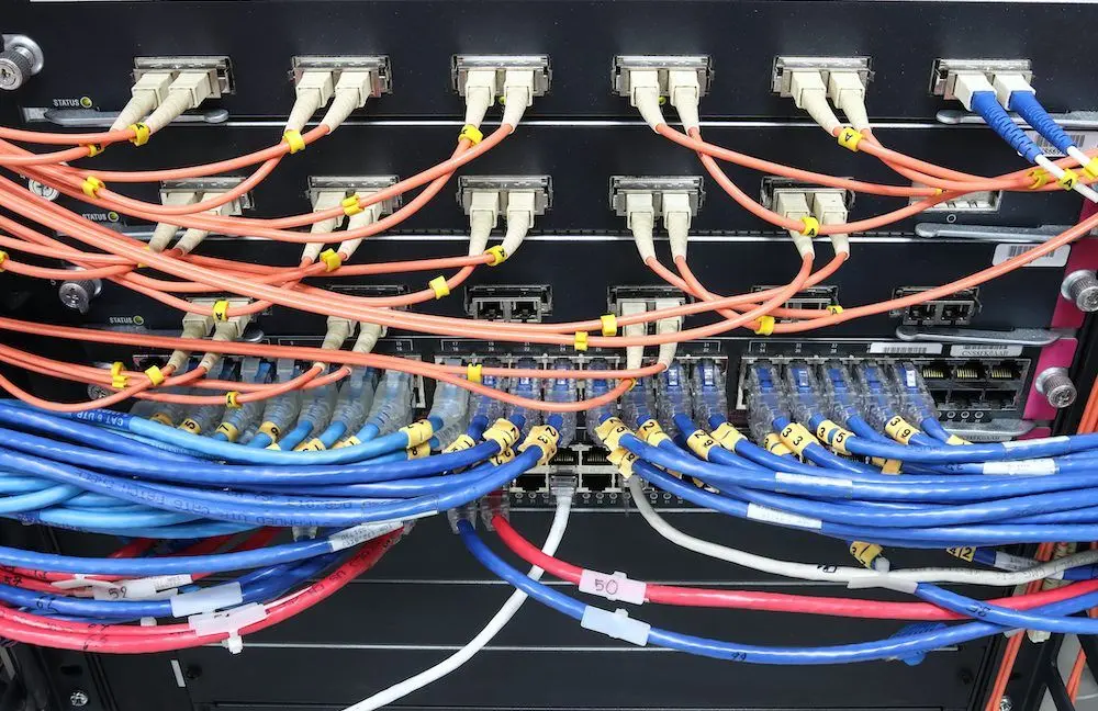
. This technology represents a fundamental shift in how AI data centers move information between processors and network infrastructure. Server switches currently represent data traffic as electrical signals, using pluggable transceivers to convert these signals into light beams for transmission over optical networks3
.Traditional architectures require traffic to move through multiple hardware componentsâfrom the processor to its substrate, then to the motherboard, and finally to a network port before reaching the transceiver. Moving traffic through these intermediate components consumes significant power and often leads to traffic errors, necessitating error correction chips that increase the cost of building optical networks
3
. Much of the supply chain for silicon photonics and advanced optical packaging is currently concentrated outside the United States, with major manufacturers including Taiwan's TSMC and Israel's Tower Semiconductor1
.

Source: Reuters
The funding will specifically support co-packaged optics, an approach that places silicon photonics circuitry in direct proximity to AI processors
2
. This technology integrates a transceiver directly into switch processors, removing the need for traffic to travel through multiple intermediate components and resulting in significant reductions in both power consumption and hardware costs3
.GlobalFoundries targets boosting data transfer speeds to 400 gigabits per second and achieving up to five times greater energy efficiency than current-generation implementations
1
4
. In May, GlobalFoundries debuted a co-packaged optics manufacturing technology called SCALE, and the company also produces other transceiver components including photodiodes and modulators3
.Related Stories

The announcement drew widespread support from major technology companies invested in AI infrastructure. NVIDIA founder and CEO Jensen Huang said in a statement that silicon photonics is "essential" to scaling U.S. manufacturing
2
. Executives from AMD, Broadcom, Cisco, Meta, Microsoft, and Qualcomm also issued statements endorsing the investment, signaling the technology's critical importance to their AI roadmaps2
.GlobalFoundries CEO Tim Breen emphasized the company's readiness to lead this transition: "Silicon photonics is essential to AI infrastructure. For a decade, the industry talked about the shift from copper to optical as something that was comingâtoday it is here, moving data at higher bandwidth and improved power efficiency as workloads grow more complex"
3
. Breen added that "GlobalFoundries has spent more than a decade building the technology, footprint and ecosystem to lead this transition, and we have the proven manufacturing foundation to scale itâin the United States"1
.
Source: SiliconANGLE
The research will leverage GlobalFoundries' facilities in Malta, New York, and Burlington, Vermont
1
4
. The company will use the federal funding to develop new optical materials, photonic wafer technologies, and advanced packaging3
. Efforts in advanced packaging will prioritize 3D hybrid bonding, a manufacturing method used to stack silicon dies atop one another3
.GlobalFoundries operates fabs that produce chips based on customer-provided designs, specializing in low-power processors that don't require the latest manufacturing technologies
3
. The development comes two months after the chipmaker secured a separate $375 million federal grant for a new quantum chip foundry3
. Watch for developments in optical chip interconnects as faster AI chip links become essential for next-generation AI processors powering increasingly complex workloads across domestic supply chains.Summarized by
Navi
05 Jun 2025â¢Business and Economy

17 Jan 2025â¢Technology

18 Nov 2025â¢Business and Economy