Google splits eighth-gen TPU into training and inference chips to challenge Nvidia dominance
24 Sources
[1]
Google unveils two new TPUs designed for the "agentic era"
Most of the companies that have fully committed to building AI models are gobbling up every Nvidia AI accelerator they can get, but Google has taken a different approach. Most of its cloud AI infrastructure is based on its line of custom Tensor processing units (TPUs). After announcing the seventh-gen Ironwood TPU in 2025, the company has moved on to the eighth-gen version, but it's not just a faster iteration of the same chip. The new TPUs come in two flavors, providing Google and its customers with an AI platform that is faster and more efficient, the company says. Google is pushing the idea that the "agent era" is fundamentally different from the AI systems that came before, necessitating a new approach to the hardware. So engineers have devised the TPU8t (for training) and the TPU 8i (for inference). Before AI models become something you can use to analyze data or make silly memes, they need to be trained. The TPU 8t was designed specifically for this part of the AI lifecycle to reduce the training time for frontier AI models from months to weeks. Updated Tensor 8t server clusters, which Google calls "pods," now house 9600 chips with two petabytes of shared high-bandwidth memory. Google claims TPU 8t can even scale linearly, with up to a million chips in a single logical cluster. It's innovations like this that are making super-sized AI models much faster while also driving up RAM prices for everyone else. But if you're involved in building those giant AI models, all this hardware saves time, with an impressive 121 FP4 EFlops of compute per pod. That's almost three times higher than Ironwood's training compute ceiling. So the new chips allow for faster training, but Google also says you get more useful computation for every volt you pump into a TPU 8t. The company claims a "goodpute" rate of 97 percent, which means less waiting and wasted effort. With better handling of irregular memory access, automatic handling of hardware faults, and real-time telemetry across all connected chips, TPU 8t spends more time actively advancing model training. When training is done, AI models run in inference mode to generate tokens -- that's the process happening behind the scenes when you tell a model to do something. This doesn't require as much horsepower, so using the same hardware for both parts of the AI lifecycle is inefficient. That's why inference is the purview of TPU 8i, which is designed to be more efficient when running multiple specialized agents, with less waiting time. TPU 8i chips also run in larger pods of 1,152 chips versus just 256 for the last-gen Ironwood inference clusters. That works out to 11.6 EFlops per pod, much lower than TPU 8t pods. Google has tripled the amount of on-chip SRAM for each TPU 8i to 384 MB. This allows the company's new chips to keep a larger key value cache on the chip, speeding up models with longer context windows. The eighth-gen AI accelerators are also the first from Google to rely solely on Google's custom Axion ARM CPU host, featuring one CPU for every two TPUs. In Ironwood, each x86 CPU serviced four TPU chips. Google says this "full-stack" ARM-based approach allows for much greater efficiency. An efficiency play It makes sense that efficiency is a core part of Google's new TPU setup. Training and running frontier AI models is expensive, and the return on investment is unclear. Companies are still burning money on generative AI in the hopes that efficiency will turn the corner at some point. Maybe Google's new TPUs will help get there and maybe not, but the company has made notable improvements. Generative AI systems consume a lot of power, which is often cited as one of the primary reasons not to use them. The eighth-gen TPUs don't exactly sip power, but Google claims the chips offer twice the performance per watt compared to Ironwood. Google also touts improvements in its data centers, which are apparently "co-designed" with TPUs. Features like integrating networking with compute on a single chip and more efficient pod layouts have reportedly increased computing power per unit of electricity by six times. Of course, that doesn't mean data centers will use less power, just that they get more compute for all the power they use. Water usage for cooling data centers is also a big efficiency concern. The heat generated by the dense computing requirements of AI servers cannot be dissipated with air, so liquid cooling is the only way. Google has adapted its fourth-gen liquid-cooling setup to the new chips, using actively controlled valves to adjust water flow based on workload. Again, this is supposed to be more efficient. The TPU 8t and TPU 8i will power Google's Gemini-based agents in the future, but they are also designed with third-party developers in mind. Both new TPUs support the frameworks developers already use, including JAX, MaxText, PyTorch, SGLang, and vLLM. Nvidia's stock price briefly dropped about 1.5 percent after Google's announcement, but it has since recovered and is again over $200 per share. Surging demand for AI accelerators has more than doubled Nvidia's value over the past year, and Google's gains have been even greater. Such is the nature of the potential AI bubble. Of course, the companies benefiting most don't see it as a bubble -- they see this as the beginning of an agentic AI future.
[2]
Google Cloud launches two new AI chips to compete with Nvidia | TechCrunch
Google Cloud on Wednesday announced that its eighth generation of custom-built AI chips, or tensor processing units (TPUs), will be split in two. One chip, named the TPU 8t, will be geared for model training and another, the TPU 8i, is aimed at inference. Inference is the ongoing usage of models, aka what happens after users submit prompts. As you might expect, the company touts some impressive performance specs for these new TPUs compared to the previous generations: up to 3x faster AI model training, 80% better performance per dollar, and the ability to get 1 million+ TPUs to work together in a single cluster. The upshot should be a lot more compute for a lot less energy -- and cost to customers -- than previous versions. It calls these chips TPUs, not GPUs, because its custom low-power chips were originally named Tensor. But Google's chips are not a full frontal assault on Nvidia's future, at least not yet. Like the other giant cloud providers, including Microsoft and Amazon, Google is using these chips to supplement the Nvidia-based systems it offers in its infrastructure. It is not flat-out replacing Nvidia. In fact, Google promises its cloud will have Nvidia's latest chip, Vera Rubin, available later this year. One day the hyperscalers building their own AI chips (which includes Amazon, Microsoft and Google) may grow to need Nvidia less, as enterprises move their AI needs to their clouds and port their apps to these chips. Still, as things stand today, it's not profitable to bet against Nvidia. As notable chip market analyst Patrick Moore jokingly posted on X, he had predicted that Google's TPU could be bad news for Nvidia (and Intel) back in 2016 when the search giant launched its first one. Nvidia is now a nearly $5 trillion market cap company, meaning that prediction didn't exactly hold up to the test of time. If all goes according to Nvidia's plan, Google's growth as an AI cloud provider would result in more business for the chip maker not less, even if many a workload runs on Google's chips. In fact, Google also says it has agreed to work with Nvidia to engineer computer networking that allows Nvidia-based systems to perform even more efficiently in its cloud. In particular, the two tech giants are working to beef up the software-based networking tech called Falcon, which Google created and open sourced in 2023 under the godfather of all open source data center hardware organizations, the Open Compute Project.
[3]
Google dual tracks TPU 8 to conquer training and inference
x86 gets the boot as Google pairs up its TPUs with some Arm-based Axion cores Google unveiled two new in-house AI accelerators at its annual Cloud Next conference in Las Vegas on Wednesday: one designed to speed up training and another aimed at driving down model serving costs. The Chocolate Factory boasts its eighth-gen tensor processing units are as much as 2.8x faster in training and deliver 80 percent higher performance per dollar for LLM inference compared with last year's Ironwood TPUs. To achieve this, Google has dual-tracked its accelerator development, building the TPU 8t for training and TPU 8i for inference. While these chips are built on similar foundations, each is specifically aimed at eliminating bottlenecks in its respective workload. Google isn't the first to go down this road. Early in its AI chip development, Amazon Web Services recognized the need for inference- and training-optimized accelerators. Nvidia has also dabbled with this kind of specialization, though not to the same extent. The GPU slinger's Blackwell Ultra generation was optimized specifically for AI inference, trading high-precision grunt for a 50 percent jump in memory and FP4 compute over its Blackwell sibling. In addition to dual tracking, Google is ditching x86 processors in favor of its homegrown Arm-based Axion CPUs for its TPU host. Amazon did something similar with Graviton and Trainium 3 earlier this year. Google's approach to specialization goes much deeper than the TPUs themselves. The search and advertising giant has developed new clusters with distinct network topologies to minimize scaling losses across both inference and training. Modern AI workloads rarely run on a single accelerator these days, so the ability to efficiently scale those workloads across multiple chips is often more important than how fast each one is. Like its past accelerators, Google's TPU 8t is designed for training at a massive scale. The company may not draw the same hype as OpenAI or Anthropic, but Google remains a prolific model builder. Under the hood, Google has tweaked the mix of vector, matrix multiplication, and SparseCore embedding accelerators introduced with its Ironwood chips to maximize effective floating point throughput. Each accelerator features 216 GB of high-bandwidth memory (HBM) good for 6.5 TB/s of bandwidth, 128 MB of on-chip SRAM, up to 12.6 petaFLOPS of 4-bit floating point compute, and up to 19.2 Tbps of chip-to-chip bandwidth. Compared to Nvidia's Rubin GPUs, which Google also announced plans to deploy across its cloud infrastructure, the new TPU might look a little tame. Rubin boasts up to 35 petaFLOPS of FP4 training performance and 288 GB of HBM4 good for 22 TB/s of bandwidth. So individually, Nvidia's GPUs are faster, but it doesn't really matter: When training a new frontier model, you're not using one GPU, you're using thousands. And when it comes to scale, Google has the advantage. Nvidia's latest GPUs support up to 576 accelerators in a single NVLink domain before having to scale out over Ethernet or InfiniBand. The TPU 8t, on the other hand, uses optical-circuit switches, an opto-mechanic switching technology that works more like a telephone switchboard than a packet switch, to connect up to 9,600 accelerators in a single unified pod. Multiple pods are then stitched together using its new Virgo Network to support even larger compute domains. Rather than just building a bigger chip-to-chip mesh, Google appears to be using packet switches with extremely high port densities. As we understand it, these are arranged in a flat-ish two-tier all-to-all topology capable of connecting up to 134,000 TPUs per datacenter and up to a million TPUs when connecting multiple sites. Or so Google claims. Alongside the new network fabric, Google has also developed a Managed Lustre storage system capable of delivering 10 TB/s of aggregate data directly into its accelerators' memory. According to Google, these technologies, combined with improved reliability, availability, and serviceability (RAS) capabilities will enable its training-optimized TPUs to operate at a "goodput" of 97 percent. In this case, goodput means the amount of time the TPUs actually spend training. "Every hardware failure, network stall, or checkpoint restart is time the cluster is not training, and at frontier training scale, every percentage point can translate into days of active training time," the company explained in a blog post. Inference is an auto-regressive workload, which means that for each token generated, the entire model's active weights need to be streamed through memory. While compute is still important, the main bottleneck tends to be memory bandwidth. For its inference-focused TPU 8i, Google is trading some FLOPS for a much larger SRAM cache and faster, higher-capacity memory pool. The chip is roughly comparable to Nvidia's Blackwell accelerators on paper. The TPU 8i features 10.1 petaFLOPS of FP4 compute fed by 384 MB of on-chip SRAM, and 288 GB of HBM good for 8.6 TB/s of bandwidth. Interconnect bandwidth, meanwhile, is unchanged from its training-focused sibling. According to Google, all that SRAM helps the TPU 8i keep more of the key-value cache (model's short term memory) resident on chip and reduce the amount of time the cores are left waiting for data. TPU 8i also ditches Google's SparseCores in favor of a collective acceleration engine (CAE). As the name suggests, the accelerator block speeds up inference by offloading collective communications, like all-reduce or all-gather, shortening synchronization stalls that would otherwise leave the chip's tensor cores sitting idle. In fact, Google's focus with TPU 8i appears to be killing as much latency across the inference stack as it can. Collective communications have become quite problematic as mixture-of-experts (MoE) architectures have become more common. These models are made up of multiple submodels, appropriately called experts, a subset of which are activated for each token generated. The benefit is models can grow larger without necessarily requiring additional memory bandwidth to maintain the same level of performance. The downside is that chip-to-chip communication is less predictable, as generating one token might use a different set of experts from the next, and those experts might be on different accelerators. Google says its CAE reduces collective communication latencies five-fold, which translates into better economics by allowing them to pack more users onto the same hardware. Alongside its inference-optimized chips, Google has also developed a topology called Boardfly. The network arrangement is somewhat reminiscent of the Dragonfly topologies commonly employed in HPC clusters, and allows 1,152 chips (1,024 active at any given moment) to be connected using optical circuit switches. The key advantage of Boardfly is it cuts the maximum chip-to-chip latency from 16 hops in a 3D torus to just seven hops, further reducing the chip-to-chip latency when running a MoE or reasoning models. Google isn't the only one that's changed the way it builds its inference clusters to better accommodate emerging architectures. In December, AWS ditched 3D toruses for inference for similar reasons, but opted instead for a more conventional packet switched fabric. Both TPU 8 accelerators will be generally available later this year in Google Cloud Platform as instances, or as part of the cloud provider's full-stack AI Hypercomputer platform, which bundles up all the networking, storage, compute, and software required to deploy or train LLMs at scale. ®
[4]
Google Cloud Releases New TPU Chip Lineup in Bid to Speed Up AI
Alphabet Inc.'s Google Cloud division unveiled the latest generation of its tensor processing unit, or TPU, a homegrown chip that's designed to make AI computing services faster and more efficient. The new lineup will come in two versions, the company said Wednesday at its Google Cloud Next event. The TPU 8t is tailored for creating artificial intelligence software, while the TPU 8i is designed to run AI services after they've been created -- a stage known as inference. Google has emerged as one of the most successful makers of in-house AI chips in an industry dominated by Nvidia Corp. TPUs have become a hot commodity in Silicon Valley in recent months, and the company is looking to build on that momentum with the latest versions. The effort is part of a broader push to make it cheaper and less energy-intensive to roll out AI software. The company also is working to make services more responsive. The new TPUs store more information on the chip, helping provide the rapid responses that users crave. But demands on increasingly complex layers of software are only growing. "It's about how you deliver the lowest possible latency of the response at the lowest possible cost per transaction," said Mark Lohmeyer, Google's vice president of compute and AI infrastructure. "The number of transactions is going way up, and the cost per transaction needs to go way down for it to scale." Creating AI services and software is done by using systems that can sift through massive amounts of data very quickly to make connections and establish patterns that can be represented mathematically. Inference, running the software and services, benefits from processors that have huge amounts of memory integrated into them. This approach helps make AI responses more instantaneous because the component doesn't have to go seek information stored elsewhere. It's particularly useful when computers "reason" through problems, taking multiple steps and learning from their own actions. Get the Tech Newsletter bundle. Get the Tech Newsletter bundle. Get the Tech Newsletter bundle. Bloomberg's subscriber-only tech newsletters, and full access to all the articles they feature. Bloomberg's subscriber-only tech newsletters, and full access to all the articles they feature. Bloomberg's subscriber-only tech newsletters, and full access to all the articles they feature. Plus Signed UpPlus Sign UpPlus Sign Up By continuing, I agree to the Privacy Policy and Terms of Service. The training chip, 8t, can be combined into groups of 9,600 semiconductors. Google said that when deploying such massive systems, power is increasingly the major constraint in data centers. Owners therefore need systems that are more efficient to get the best out of the limited availability of electricity. TPU 8t delivers 124% more performance per watt than the preceding generation, with TPU 8i providing a gain of 117%. That step-up is helped by improving in-house networking that increases the chips' ability to communicate with one another efficiently. AI systems built on the chips will be "generally available later this year," Google said in a statement. The company will continue to offer services based on Nvidia chips to customers who want to use the systems that currently dominate AI computing, it said. Google intends to be among the first to deploy gear based on a new design from Nvidia coming in the second half of the year, Lohmeyer said. Like Google, Nvidia is focusing more on the inference stage of AI. Its forthcoming lineup will include technology from its acquisition of Groq -- technology tailored specifically for providing ultrafast responsiveness. Nvidia Chief Executive Officer Jensen Huang has said that more than 20% of AI workloads might be best served by that type of chip. Groq was founded in 2016 by a group of former Google engineers. Last December, Nvidia paid $20 billion for a license to use its technology and hired most of its engineering team.
[5]
Google unveils chips for AI training and inference in latest shot at Nvidia
Google CEO Sundar Pichai gestures during a meeting with France's President Emmanuel Macron on the sidelines of the AI Impact Summit in New Delhi on Feb. 19, 2026. After years of producing chips that can both train artificial intelligence models and handle inference work, Google is separating those tasks into distinct processors, its latest effort to take on Nvidia in AI hardware. Google said Wednesday that it's making the change for the eighth generation of its tensor processing unit, or TPU. Both chips will become available later this year. "With the rise of AI agents, we determined the community would benefit from chips individually specialized to the needs of training and serving," Amin Vahdat, a Google senior vice president and chief technologist for AI and infrastructure, said in a blog post. In March, Nvidia talked up forthcoming silicon that can enable models to rapidly respond to users' questions, thanks to technology obtained in its $20 billion deal with chip startup Groq. Google is a large Nvidia customer, but offers TPUs as an alternative for companies that use its cloud services. Most of the world's top technology companies are pursuing custom semiconductor development for artificial intelligence to maximize efficiency and so they can build for specialized use cases. Apple has included neural engine AI components in its in-house iPhone chips for years. Microsoft announced a second-generation AI chip in January. Last week, Meta said it's working with Broadcom to develop multiple versions of AI processors. Google was early to the trend. In 2015, the company started using processors it had designed for running AI models, and began renting them to cloud clients in 2018. Amazon Web Services announced the Inferentia chip for handling AI requests in 2018, and unveiled the Trainium processor for training AI models in 2020. DA Davidson analysts estimated in September that the TPU business, coupled with the Google DeepMind AI group, would be worth about $900 billion. None of the tech giants are displacing Nvidia, and Google isn't even comparing the performance of its new chips with those from the AI chip leader. Google did say the training chip enables 2.8 times the performance of the seventh-generation Ironwood TPU, announced in November, for the same price, while performance is 80% better for the inference processor. Nvidia said its upcoming Groq 3 LPU hardware will draw on large quantities of static random-access memory, or SRAM, which is used by Cerebras, an AI chipmaker that filed to go public earlier this month, Google's new inference chip, dubbed TPU 8i, also relies on SRAM. Each chip contains 384 MB of SRAM, triple the amount in Ironwood. The architecture is designed "to deliver the massive throughput and low latency needed to concurrently run millions of agents cost-effectively," Sundar Pichai, CEO of Google parent Alphabet, wrote in a blog post. Adoption of Google's AI chips is ramping up. Citadel Securities built quantitative research software that draws on Google's TPUs, and all 17 U.S. Energy Department national laboratories use AI co-scientist software built on the chips, Google said. Anthropic has committed to using multiple gigawatts worth of Google TPUs.
[6]
Google Eyes New Chips to Speed Up AI Results, Challenging Nvidia
In a matter of months, Google's AI chips have become one of the hottest commodities in the tech sector. Leading artificial intelligence developers, including some of the firm's biggest rivals, are stocking up on them. Now, the Alphabet Inc.-owned company aims to build on its momentum with the likely introduction of new chips dedicated to inference, or running AI models after they've been trained. With this push, Google is poised to further challenge market leader Nvidia Corp. in a fast-growing category for semiconductors that's fueled by surging adoption of AI software. As demand grows for quickly processing AI queries, "it now becomes sensible to specialize chips more for training or more for inference workloads," Google Chief Scientist Jeff Dean said in an interview. "We are looking at a whole bunch of different things," he added, including the speed of AI results it wants to enable. The company plans to announce its new generation of custom-designed chips, known as tensor processing units, or TPUs, at the Google Cloud Next conference in Las Vegas this week. Amin Vahdat, who oversees Google's AI infrastructure and chip work, declined to comment on plans for an inference chip that can speed up AI outputs, but said more will likely be shared "in the relatively near future." Nvidia's graphics processing units, or GPUs, remain the gold standard for AI, particularly for training more advanced models. But a growing number of up-and-comers are vying to take on the chipmaker for inference uses, including by offering chips meant to cut down response times for chatbots and AI agents. Last month, Nvidia began selling a chip intended for faster inference based on technology it acquired from Groq as part of a reported $20 billion licensing deal. Google brings unique strengths to that competitive landscape, including a decade of experience designing chips, vast resources from its online search profits and firsthand insights on AI models. Among the top AI developers, only Google makes its own chips at significant scale, allowing it to share vital feedback between teams to better customize hardware. (OpenAI is only now starting to design its own.) In a recent podcast interview, Nvidia's Jensen Huang stressed the advantages of his company's chips, saying they can do "a whole bunch of applications" that "you can't do with TPUs." Google, for its part, relies on a mix of TPUs and GPUs for its own work. "A lot of people would like to run on both," Demis Hassabis, chief executive officer of Google DeepMind, told Bloomberg. Interest in TPUs is particularly high from leading AI labs, he said. Google has previously touted inference capabilities for its chips. It also considered releasing separate chips for training and inference early on, according to Partha Ranganathan, a vice president and engineering fellow at Google, but so far it's resisted that approach. That might change soon as the AI spending boom moves from training to inference. "The battleground is shifting towards inference," said Chirag Dekate, an analyst at Gartner, who notes that in his experience Google's Gemini model is the fastest at responding to complex reasoning tasks. "In that battleground, Google has an infrastructure advantage." Already, today's TPUs are a strong choice for processing results for the emerging crop of AI agents that field more complex work on a user's behalf, according to Natalie Serrino, co-founder at Gimlet Labs, a startup that makes software for routing AI tasks to the best chip for each job. "They are very good tools for the workload that is exploding," she said. An overnight success that took a decade Google's long-simmering chip efforts gained new attention in October when Anthropic PBC -- one of the most closely watched AI developers -- unveiled an expanded agreement to access as many as 1 million TPUs. The next month, Google debuted the more advanced Gemini 3 model, trained and run on TPUs, to rave reviews. Since then, demand for Google's chips has only grown among large firms. Meta Platforms Inc. signed a multibillion-dollar deal to use TPUs through Google Cloud over several years. The company just received access to its first significant supply and is testing them out to see what tasks they're best suited for, said Santosh Janardhan, Meta's head of infrastructure. "It does look like there might be inference advantages," he said, while noting that "no new platform is without hurdles and a learning curve." Anthropic also signed a deal with Broadcom Inc., Google's TPU partner, for chips that will enable it to tap into about 3.5 gigawatts of computing power starting in 2027. Citadel Securities plans to present at the Google conference about how TPUs let the company train models faster than previous work with GPUs. And G42, the Abu Dhabi technology conglomerate, has held "multiple discussions" with Google about using its TPUs, according to Talal Al Kaissi, the interim CEO of Core42, the firm's cloud unit. "I'm very bullish," Al Kaissi said about the talks. Google is already taking new steps to meet customers where they are. The company is testing out letting companies like Anthropic run some of their TPUs in their own data centers rather than Google's facilities, according to a person familiar with the matter. It has also enabled TPU customers to use outside tools like PyTorch as well as other scheduling software rather than solely relying on Google's products, Vahdat said. Those changes are helping shift perception for chips that were born out of Google's computing bottlenecks and long thought of as primarily useful for the company to meet its own needs. After Dean, Google's chief scientist, started building an earlier AI software system to let people use language translation and voice recognition services, he realized there was no way that even Google could afford to deliver it using available chips and hardware. At the same time, the central processing units Google relied on for AI were improving at a slower rate. The company decided it should build an accelerator that focused on a narrower set of tasks that might rack up the biggest bills for AI. The key idea behind the TPU is that it "solves a small number of problems but the amount of computation required for them was enormous," said Vahdat, a former computer science professor who played an early, key role in pushing Google to adopt the optical switches that help connect TPUs into supercomputers. "The conventional wisdom at the time was you don't build specialized hardware." Over the years, Google's TPUs have evolved alongside its AI work. A seminal 2017 Google research paper that gave rise to today's large language models also pushed the TPU team to focus on chips for training bigger AI systems. Later, Google DeepMind and the chips team noticed that TPUs were sitting unused too often when deployed for reinforcement learning, a popular method for improving AI systems at specific tasks. The TPU team adjusted how they network various semiconductors to get the data flowing faster and avoid chips sitting idle. That dynamic continues today as Google debates how many chips to link together in a single pod or whether the hardware can be less precise in order to save money. "A lot of those things are informed by the model experiments," Hassabis said. In the future, he would love the TPU team to consider making an accelerator for edge-of-network cases, where the chip is placed closer to users, rather than being accessed via the cloud to reduce latency. Along the way, Google has also built systems to more rapidly spot manufacturing flaws that can have an outsize impact on software. When working with AI accelerator chips that manage massive amounts of math, even a subtle failure can metastasize and cause a model to "completely self-destruct," said Paul Barham, the Google distinguished scientist who co-leads the Gemini infrastructure team. An issue like that happened at Google about two years ago and took weeks to sort out what happened, he said, describing these as "bugs from hell." "We now have to do that with hundreds of thousands of accelerator chips within 10 seconds," he said. The guessing game For all its expertise in AI development, Google faces a similar challenge to other chipmakers: Chips usually take about three years to develop from start to finish, but AI models are evolving much faster. That makes it difficult to predict what customers will want several years out. "If anybody claims they know what Gemini 10 is going to look like, I'm like, 'Please give me whatever you're smoking,'" Ranganathan said. Barham also worries that the tight feedback loop between the AI model creators and the hardware designers can run the risk of missing new ideas. There's "this cycle that traps you into what works well on the current software and hardware," he said. To strike a middle ground, the TPU team sometimes aims for the chip to be good enough for various uses, even if it's not perfect for each. The other option, Vahdat said, is to plan two different designs. Both may not ship, but they could if the use case for each is compelling enough. As Google's chips become more popular, the company risks supply constraints, not unlike Nvidia. One startup executive, who spoke on condition of anonymity to discuss internal matters, said their company's use of TPUs has been limited by availability and complained that Google had effectively given all its chips to Anthropic. "Mostly we're sort of favoring what supply we do have to the more elite teams who obviously are the ones that could maybe take the most advantage out of what the TPUs do best," Hassabis said, referring to top AI firms. Going forward, Google will also need to decide how to allocate TPUs between its own growing slate of competitive AI services and its burgeoning roster of customers. "There are benefits to making TPUs only for Google, but there are substantial downsides," Vahdat said. "Eventually you wind up on what we refer to as a tech island. It might be a beautiful island, but it's going to be limited in population and it's going to be limited in diversity. In the end, it's probably going to be less good."
[7]
Google launches Ironwood TPU and previews eighth-gen split into training and inference chips at TSMC 2nm
Summary: Google made Ironwood, its seventh-generation TPU, generally available at Cloud Next 2026 while previewing its eighth-generation architecture: TPU 8t (Sunfish), a Broadcom-designed training chip, and TPU 8i (Zebrafish), a MediaTek-designed inference chip, both targeting TSMC 2nm and late 2027. Ironwood delivers 4.6 petaFLOPS per chip and 42.5 exaFLOPS in a 9,216-chip superpod. The v8 split marks the first time Google has purpose-built separate training and inference chips, with Anthropic's deal expanding to 3.5 gigawatts of compute in 2027, making it the anchor customer for both generations. Google made its seventh-generation Tensor Processing Unit, Ironwood, generally available to cloud customers on Tuesday at Google Cloud Next in Las Vegas, positioning the chip as "the first Google TPU for the age of inference" and the centrepiece of what may be the most aggressive infrastructure investment in the company's history. Ironwood delivers 4.6 petaFLOPS of peak FP8 compute per chip, roughly four times the performance of its predecessor Trillium, with 192 gigabytes of HBM3e memory and 7.37 terabytes per second of memory bandwidth. A single Ironwood superpod links 9,216 chips into a unified system delivering 42.5 exaFLOPS of compute, more than 24 times the capacity of El Capitan, currently the world's most powerful supercomputer. The numbers position Ironwood as a direct competitor to Nvidia's Blackwell B200 on raw specifications. Both chips deliver roughly 4.5 to 4.6 petaFLOPS of FP8 compute and 192 gigabytes of HBM. Nvidia leads on single-device interconnect bandwidth, 14.4 terabits per second via NVLink compared with Ironwood's 9.6 terabits over ICI, and supports FP4 precision, which doubles inference throughput for quantised models, a capability Ironwood lacks. Google's advantage is at cluster scale: the superpod architecture, its energy efficiency at roughly twice the performance per watt of Trillium and 2.8 times that of Nvidia's H100, and the economics of running inference workloads on custom silicon designed specifically for the task rather than on general-purpose GPUs adapted for it. The emphasis on inference rather than training marks a strategic shift. Training a frontier model is a one-time capital expenditure measured in weeks or months. Inference, the process of running that model in response to every query from every user, is an ongoing operational cost that scales with demand and never stops. Google says it must double its AI serving capacity every six months to meet demand across Gemini, Search, YouTube, and Gmail. At that growth rate, the cost of inference becomes the single largest variable in the economics of AI, and the company that builds the cheapest, most efficient inference hardware captures the margin that would otherwise flow to Nvidia. Ironwood is Google's answer. It is purpose-built for the workloads that dominate production AI: large language model inference, mixture-of-experts architectures, diffusion models, and reinforcement learning. Its 192 gigabytes of HBM3e per chip allow it to hold larger model shards in memory, reducing the need to distribute a single model across multiple chips. Its 256-by-256 matrix multiply unit array, containing 65,536 multiply-accumulate operations per cycle, is optimised for the dense linear algebra that accounts for most of the compute in transformer inference. Google is also making its internal Pathways distributed runtime available to cloud customers for the first time, enabling multi-host inference with dynamic scaling across Ironwood pods. Alongside Ironwood's general availability, Google previewed its eighth-generation TPU architecture, and for the first time, it is splitting the line in two. TPU 8t, codenamed Sunfish, is a training accelerator designed with Broadcom. It features two compute dies, one I/O chiplet, and eight stacks of 12-high HBM3e, an upgrade from Ironwood's eight-high stacks that delivers roughly 30% higher memory bandwidth. TPU 8i, codenamed Zebrafish, is an inference accelerator designed with MediaTek. It uses a single compute die, one I/O die, and six stacks of HBM3e, a simpler configuration engineered to deliver inference at 20 to 30% lower cost than the training variant. Both chips will be fabricated on TSMC's 2-nanometre process node and are targeted for late 2027. The bifurcation is the most significant architectural decision in Google's TPU history. Every previous generation was a unified chip used for both training and inference. Splitting the two acknowledges a reality the industry has been approaching for years: the workloads are fundamentally different. Training demands maximum compute density and memory bandwidth to process trillions of parameters across weeks of continuous operation. Inference demands cost efficiency and low latency to serve billions of queries per day without the economics collapsing. Designing one chip that is optimal for both has always been a compromise. Google has decided to stop compromising. The decision also locks in the multi-supplier strategy. Broadcom handles the high-performance training silicon under a relationship that has been described as a $46 billion AI contract. MediaTek handles cost-optimised inference, having already proved its ability to deliver I/O modules for Ironwood at 20 to 30% lower cost than alternatives. MediaTek has reportedly requested a sevenfold increase in CoWoS advanced packaging capacity from TSMC to fulfil Google's orders. Anthropic, whose deal has expanded to 3.5 gigawatts of compute coming online in 2027, will be among the first customers for both variants. The eighth-generation roadmap makes explicit what Ironwood's general availability already implied: Google is building the AI industry's most diversified custom chip supply chain. Broadcom designs Ironwood and the TPU 8t training chip under an agreement running through 2031. MediaTek designs the TPU 8i inference chip and cost-optimised variants including TPU v7e and v8e. Google is in talks with Marvell to develop a memory processing unit and another inference-focused TPU, potentially becoming the third design partner. Intel provides CPUs and is collaborating on custom IPU development. The multi-supplier approach gives Google negotiating leverage, supply chain redundancy, and the ability to assign each partner the workload profile that matches its strengths. Google projects 4.3 million TPU shipments in 2026, rising to 10 million in 2027 and more than 35 million in 2028. The capital expenditure to support this is enormous. Google has committed $175 billion to $185 billion in infrastructure spending for 2026, nearly doubling the $91.4 billion it spent in 2025, itself a figure that was revised upward twice during the year. Roughly 60% goes to servers and 40% to data centres and networking equipment. Combined with Microsoft, Meta, and Amazon, total big tech AI infrastructure spending is approaching $700 billion this year. Anthropic is Ironwood's marquee customer and increasingly Google's most important cloud client. The company will have access to up to one million TPU chips and more than a gigawatt of capacity in 2026. The first phase covers 400,000 Ironwood units, worth an estimated $10 billion in finished racks from Broadcom. The remaining 600,000 units are rented through Google Cloud Platform. The partnership has already expanded: Anthropic's deal now covers 3.5 gigawatts of compute coming online in 2027, positioning it as the anchor customer for the eighth-generation TPUs as well. Anthropic's run-rate revenue has surpassed $30 billion, up from roughly $9 billion at the end of 2025, and it described itself as "compelled by the impressive price-performance gains." It maintains a diversified compute strategy that also includes Amazon Trainium and Nvidia GPUs. The fact that Anthropic is even exploring designing its own custom chips while simultaneously committing to a multi-gigawatt Google TPU deployment illustrates both the scale of inference demand and the degree to which the economics of AI hardware have become a competitive variable in their own right. Ironwood reaches general availability roughly one year after Nvidia's Blackwell architecture. In that year, every major cloud provider has accelerated its custom silicon programme. Amazon values its custom chip business at $50 billion and has hinted at selling Trainium externally. Microsoft's Maia 200, announced in January, claims three times the FP4 performance of Amazon's Trainium 3. Meta continues developing MTIA. The custom ASIC market for AI is growing at 44.6% annually, compared with 16.1% for GPUs. Analysts project that custom chips could account for 45% of the AI chip market by 2028, and that Nvidia's share of the inference market specifically could fall from more than 90% to between 20 and 30%. Nvidia's response has been to lock in the ecosystem through NVLink Fusion, a strategy that makes its interconnect the default standard for custom silicon, including chips designed to compete with Nvidia's own GPUs. Jensen Huang has brushed off the custom chip threat with characteristic confidence: "Not that easy building something better." He is not wrong that Nvidia's CUDA software ecosystem, developer tools, and interconnect standards create switching costs that raw hardware specifications do not capture. But the direction of the market is clear. The hyperscalers are building their own chips not because they think they can beat Nvidia on every metric but because they have concluded that purpose-built inference silicon, optimised for their specific workloads and deployed at their specific scale, produces better economics than buying Nvidia GPUs at Nvidia's margins. Google Cloud holds roughly 11% of the cloud infrastructure market, behind AWS at 31% and Azure at 25%, but exited 2025 with the fastest growth rate among the three and its first sustained period of profitability. Ironwood does not change Google's position in the cloud market overnight, and Nvidia's Rubin architecture, also targeting late 2027, may reclaim performance advantages in memory and networking that could shift total cost of ownership calculations back in its favour. But the direction Google has committed to is now irreversible: a roadmap stretching from Ironwood shipping today through two purpose-built eighth-generation chips at 2 nanometres in 2027, backed by $185 billion in annual infrastructure spending, a four-partner supply chain, and an anchor customer in Anthropic that is scaling to 3.5 gigawatts. The chip race is, in the end, a margin race. Google is betting that the margin belongs to the company that builds the silicon, not the company that buys it, and it is now building two chips where it used to build one.
[8]
Google launches TPU 8 chips to speed AI training and cut costs
Google said TPU 8t targets more than 97 percent "goodput," a term used to measure productive compute time instead of idle time caused by failures or bottlenecks. That matters because delays across massive clusters can add days to training schedules for advanced AI systems. The TPU 8i focuses on inference, the stage where trained AI models answer prompts, run tools, and power software agents. Google said TPU 8i includes 288 GB of high-bandwidth memory and 384 MB of on-chip SRAM, helping keep active model data closer to the processor for faster responses. The chip also uses Google's Axion Arm-based CPUs and upgraded interconnect bandwidth for Mixture of Experts, or MoE, models. These architectures activate only parts of a model at a time to lower costs while scaling performance. According to Google, TPU 8i delivers 80% better performance-per-dollar than the prior generation, allowing customers to handle nearly twice the workload at the same cost. The launch highlights how AI infrastructure is shifting beyond general-purpose GPUs toward specialized chips tuned for different workloads.
[9]
Google assembles four-partner chip supply chain with Broadcom, MediaTek, Marvell to challenge Nvidia in inference
Summary: Google is building the AI industry's most diversified custom chip supply chain, with four design partners (Broadcom, MediaTek, Marvell, Intel) and a roadmap stretching from the Ironwood TPU now shipping in the millions to TPU v8 chips at TSMC 2nm in late 2027. The strategy, detailed ahead of Google Cloud Next, splits the next generation explicitly: Broadcom's "Sunfish" for training, MediaTek's "Zebrafish" for inference at 20-30% lower cost, with Marvell in talks to add a memory processing unit and an additional inference TPU, positioning Google's custom silicon as the most direct challenge to Nvidia's dominance in AI inference. Google is assembling the most diversified custom chip supply chain in the AI industry, with four design partners, a fabrication relationship with TSMC, and a product roadmap that now stretches from the inference chips it is shipping today to the 2-nanometre processors it expects to deploy in late 2027. The strategy, detailed in a Bloomberg feature ahead of Google Cloud Next this week, positions Google's silicon programme as the most direct challenge to Nvidia's dominance in AI inference, the phase of computing where models serve users rather than learn from data. The centrepiece is Ironwood, Google's seventh-generation TPU and the first designed specifically for inference. It delivers ten times the peak performance of the TPU v5p, offers 192 gigabytes of HBM3E memory per chip with 7.2 terabytes per second of bandwidth, and scales to 9,216 liquid-cooled chips in a single superpod producing 42.5 FP8 exaflops. Ironwood is now generally available to Google Cloud customers. Google plans to produce millions of units this year, and Anthropic has committed to up to one million TPUs. Meta also has a rental arrangement. Google's chip programme now involves four distinct design partners, each handling different segments of the product line. Broadcom, which signed a long-term agreement on 6 April to supply TPUs and networking components through 2031, handles the high-performance chip variants. It is also designing the next-generation TPU v8 training chip, codenamed "Sunfish," targeted at TSMC's 2-nanometre process node for late 2027. Broadcom commands more than 70% of the custom AI accelerator market and is projecting $100 billion in AI chip revenue by 2027. MediaTek is designing the cost-optimised inference variant of the TPU v8, codenamed "Zebrafish," also targeting TSMC 2nm in late 2027. MediaTek's involvement began with the I/O modules and peripheral components on Ironwood, where its designs run 20 to 30% cheaper than alternatives. The TPU v8 strategy splits the product line explicitly: Broadcom builds the training chip, MediaTek builds the inference chip, and Google gains the negotiating leverage that comes from having each partner know the other exists. Marvell Technology, which is in talks with Google to develop a memory processing unit and a new inference-focused TPU, would become the third design partner if those negotiations produce a contract. Google plans to produce nearly two million of the memory processing units, with design finalisation expected by next year. Marvell's custom silicon business runs at a $1.5 billion annual rate across 18 cloud-provider design wins, and Nvidia invested $2 billion in the company in March. Intel entered the picture on 9 April with a multi-year deal to supply Xeon processors and custom infrastructure processing units for Google's AI data centre infrastructure. The arrangement covers the networking and general-purpose compute layers that surround the TPUs rather than the AI accelerators themselves. TSMC fabricates all of Google's custom silicon. The relationship is structural: every chip Google designs, regardless of which partner designed it, runs through TSMC's fabs. The shift from training to inference as the dominant AI compute cost is the strategic premise behind Google's entire chip programme. Training a frontier model is a singular, intensive event. Inference is continuous and scales with every user, every query, and every product that incorporates AI. Google serves billions of AI-augmented search queries, Gemini conversations, and Cloud AI API calls daily. At that scale, the cost per inference determines the economics of the entire AI business. Nvidia's GPUs remain dominant for training workloads, where their programmability and the CUDA software ecosystem create switching costs that custom chips cannot easily replicate. But inference workloads are more predictable, more repetitive, and more amenable to the kind of fixed-function optimisation that custom silicon excels at. A purpose-built inference chip that costs less per query than an Nvidia GPU, even if it cannot match the GPU's versatility, wins on the metric that matters at Google's scale. This is why Google is investing in multiple inference chip paths simultaneously. Ironwood serves today's workloads. MediaTek's Zebrafish targets the next generation at lower cost. Marvell's proposed chips would add yet another option. The redundancy is deliberate: Google is building optionality into a supply chain where dependence on any single partner creates pricing risk, capacity risk, and the strategic vulnerability of having its AI infrastructure controlled by someone else's roadmap. Google's total expected TPU shipments are projected at 4.3 million units in 2026, scaling to more than 35 million by 2028. Anthropic's commitment alone represents up to one million of those chips, with access to approximately 3.5 gigawatts of next-generation TPU-based compute starting in 2027. Broadcom's Mizuho-estimated AI revenue from its Google and Anthropic relationships is $21 billion in 2026, rising to $42 billion in 2027. The custom ASIC market more broadly is growing faster than GPUs. TrendForce projects custom chip sales will increase 45% in 2026, compared with 16% growth in GPU shipments. The market is expected to reach $118 billion by 2033. Google is not the only hyperscaler building custom inference silicon: Amazon has Trainium and Inferentia, Microsoft has Maia, and Anthropic is exploring its own chip programme. But Google's multi-partner, multi-generation approach is the most architecturally ambitious. Google Cloud Next opens on Wednesday in Las Vegas with keynotes from Sundar Pichai and Thomas Kurian. The conference is expected to showcase the next-generation TPU architecture and the custom silicon roadmap that connects Ironwood to the v8 generation. The timing of the Bloomberg feature, one day after The Information broke the Marvell talks and two days before Cloud Next, suggests Google is using the conference to frame its chip programme as a coherent strategy rather than a series of individual partnerships. The challenge Nvidia faces is not that any single Google chip will outperform its GPUs. It is that Google is building a system in which multiple custom chips, each optimised for a specific workload and cost point, collectively reduce the share of Google's AI compute that runs on Nvidia hardware. Nvidia's response has been to embed itself in the custom chip ecosystem rather than fight it: the $2 billion Marvell investment and the NVLink Fusion programme ensure Nvidia retains a position in racks where its GPUs are supplemented or replaced by ASICs. For Google, the bet is that controlling its own silicon, across multiple partners and multiple generations, will produce a cost advantage in inference that compounds over time. The scale of Nvidia's business means the incumbent will not be displaced quickly. But the economics of inference favour custom silicon over general-purpose GPUs, and no company has more inference volume than Google. The four-partner supply chain, the dual-track v8 roadmap, and the millions of Ironwood chips shipping this year are the infrastructure for a competitive position that Google expects to strengthen with every query it serves.
[10]
Google Cloud unveils eighth-generation TPUs built to support an agentic era
* Google unveils next-generation TPUs - splits off into two series, 8t and 8i * 8t superpods can deliver 121 ExaFlops, up from 42.5 last year * 8i delivers 3x more SRAM and increased HBM Google Cloud has announced its eighth-generation Tensor Processing Units (TPUs) designed specifically for the agentic shift we're seeing within AI at the moment. Revealed at Google Cloud Next 2026, the upgrades focus on longer context windows, multi-step reasoning and responsiveness at scale, thus its cloud infrastructure is being rebuilt to support persistent memory, continuous inference and multi-model workloads. This year, we're seeing two distinct TPUs designed to support massive HBM scaling, with Google Cloud placing an emphasis on memory bandwidth as much as compute. TPU 8t and 8i target trillion-parameter training in million-chip clusters The first of two TPUs, 8t, has been optimized to be distributed across huge clusters for training foundation models. With around an 80% year-over-year improvement in performance per dollar, the company says it will train trillion-parameter models more efficiently. Google Cloud explained that a single TPU 8t superpod can scale up to 9,600 chips, delivering 2PB of shared HBM and 121 ExaFlops of compute. For comparison, last year Ironwood was rated at up to 9,216 chips in a superpod and 42.5 ExaFlops. Google Cloud also warned of "the latency wall" we face in an always-on agentic era, hence the launch of 8i, a second chip which serves as a post-training and inference engine. TPU 8i sees around a 3x increase in on-chip SRAM to 384MB as well as 288GB of HBM, with pod size now up to 1,152 chips from 256, delivering 11.6 ExaFlops of performance (up from 1.2 ExaFlops). As for energy and thermal efficiency, Google Cloud boasts of up to 2x better performance-per-watt over Ironwood, the predecessor. "We['ve] innovated across hardware and software to enable our data centers to deliver six times more computing power per unit of electricity than they did just five years ago," SVP and Chief Technologist for AI and Infrastructure Amin Vahdat explained. General availability for Google Cloud customers is expected in the coming months, and naturally, TPU 8t and TPU 8i will be at the forefront of the latest Gemini models. The company also sees the eighth-gen hardware playing a role in developing the next frontier models by distributing training beyond a single superpod using Pathways and JAX to unlock scaling beyond one million TPU chips per any single training cluster - something execs confirmed at the event is currently entirely theoretical (but technically possible), with the TPUs yet to be made available at such a scale. Follow TechRadar on Google News and add us as a preferred source to get our expert news, reviews, and opinion in your feeds. Make sure to click the Follow button! And of course you can also follow TechRadar on TikTok for news, reviews, unboxings in video form, and get regular updates from us on WhatsApp too.
[11]
Google doesn't pay the Nvidia tax. Its new TPUs explain why.
Every frontier AI lab right now is rationing two things: electricity and compute. Most of them buy their compute for model training from the same supplier, at the steep gross margins that have turned Nvidia into one of the most valuable companies in the world. Google does not. On Tuesday night, inside a private gathering at F1 Plaza in Las Vegas, Google previewed its eighth-generation Tensor Processing Units. The pitch: two custom silicon designs shipping later this year, each purpose-built for a different half of the modern AI workload. TPU 8t targets training for frontier models, and TPU 8i targets the low-latency, memory-hungry world of agentic inference and real-time sampling. Amin Vahdat, Google's SVP and chief technologist for AI and infrastructure (pictured above left), used his time onstage to make a point that matters more to enterprise buyers than any individual spec: Google designs every layer of its AI stack end-to-end, and that vertical integration is starting to show up in cost-per-token economics that Google says its rivals cannot match. The more interesting story behind v8t and v8i is when the decision to split the roadmap was made. The call came in 2024, according to Vahdat -- a year before the industry at large pivoted to reasoning models, agents and reinforcement learning as the dominant frontier workload. At the time, it was a contrarian read. "We realized two years ago that one chip a year wouldn't be enough," Vahdat said during the fireside. "This is our first shot at actually going with two super high-powered specialized chips." For enterprise buyers, the implication is concrete. Customers running fine-tuning or large-scale training on Google Cloud and customers serving production agents on Vertex AI have been renting the same accelerators and eating the inefficiency. V8 is the first generation where the silicon itself treats those as different problems with two sets of chips. On paper, TPU 8t is an aggressive generational step. According to Google, 8t delivers 2.8x the FP4 EFlops per pod (121 vs 42.5) against Ironwood, the seventh-generation TPU that shipped in 2025, doubles bidirectional scale-up bandwidth to 19.2 Tb/s per chip, and quadruples scale-out networking to 400 Gb/s per chip. Pod size grows modestly from 9,216 to 9,600 chips, held together by Google's 3D Torus topology. The number that matters most to IT leaders evaluating where to run frontier-scale training: 8t clusters (Superpods) can scale beyond 1 million TPU chips in a single training job via a new interconnect Google is calling Virgo networking. 8t also introduces TPU Direct Storage, which moves data from Google's managed storage tier directly into HBM without the usual CPU-mediated hops. For long training runs where wall-clock time is the cost driver, collapsing that data path reduces the number of pod-hours needed to finish each epoch. If 8t is an evolutionary step, TPU 8i is the more architecturally interesting chip. It is also where the story for IT buyers gets most compelling. The year-over-year spec jumps are, as Vahdat put it, "stunning." According to Google, 8i delivers 9.8x the FP8 EFlops per pod (11.6 vs 1.2), 6.8x the HBM capacity per pod (331.8 TB vs 49.2), and a pod size that grows 4.5x from 256 to 1,152 chips. What drove those numbers is a rethink of the network itself. Vahdat explained the insight directly: Google's default way of connecting chips together supported bandwidth over latency -- good for moving large amounts of data through, not built for the minimum time it takes a response to get back. That profile works for training. For agents, it does not. In partnership with Google DeepMind, the TPU team built what Google calls Boardfly topology specifically to reduce the network diameter -- shrinking the number of hops between any two chips in a pod. Paired with a Collective Acceleration Engine and what Google describes as very large on-chip SRAM, 8i delivers a claimed 5x improvement in latency for real-time LLM sampling and reinforcement learning. The subtext across Vahdat's presentation was a six-layer diagram Google calls its AI stack: energy at the foundation, then data center land and enclosures, AI infrastructure hardware, AI infrastructure software, models (Gemini 3), and services on top. Vahdat noted that designing each layer in isolation forces you to the least common denominator for each layer. Google designs them together. This is where the competitive story for IT buyers and analysts crystallizes. OpenAI, Anthropic, xAI and Meta all depend heavily on Nvidia silicon to train their frontier models. Every H200 and Blackwell GPU they buy carries Nvidia's data-center gross margin -- the informal "Nvidia tax" that industry analysts have flagged for two years running as a structural cost disadvantage for anyone renting rather than designing. Google pays fab, packaging and engineering costs on its TPUs. It does not pay that margin. For procurement and infrastructure teams, TPUv8 reframes the 2026-2027 cloud evaluation in concrete ways. Teams training large proprietary models should look at 8t availability windows, Virgo networking access, and goodput SLAs -- not just headline EFlops. Teams serving agents or reasoning workloads should evaluate 8i availability on Vertex AI, independent latency benchmarks as they emerge, and whether HBM-per-pod sizing fits their context windows. Teams consuming Gemini through Gemini Enterprise should inherit the 8i lift and should expect the ceiling on what they can deploy in production to rise meaningfully through 2026. The caveats are real. General availability is still "later in 2026." The v8 is a roadmap signal, not a procurement decision today. Google's benchmarks are self-reported; undoubtedly independent numbers will come from early cloud customers and third-party evaluators over the next two quarters. And portability between JAX/XLA and the CUDA/PyTorch ecosystem remains a friction cost worth thinking about when negotiating any multi-year commitment. Looking further out, Vahdat made two predictions worth noting. First, general-purpose CPUs will see a resurgence inside AI systems -- not as accelerators, but as orchestration compute for agent sandboxes, virtual machines and tool execution. Second, framed explicitly as an industry prediction rather than a Google roadmap preview, specialization also keeps going strong. As general-purpose CPUs gain plateau at a few percent a year, workloads that matter will demand purpose-built silicon. "Two chips might become more," Vahdat said -- without specifying whether the "more" would mean future TPU variants or other classes of specialized accelerators. The frontier compute race used to be a question of who could buy the most H100s. It is now a question of who controls the stack. The shortlist of companies that genuinely do is, for the moment, two: Google and Nvidia.
[12]
Google developing inference AI chips to rival Nvidia
Google $GOOGL is developing new chips dedicated to AI inference in partnership with Marvell Technology, positioning Alphabet to more directly compete with Nvidia $NVDA in a semiconductor category driven by surging demand for AI software, according to Bloomberg. After a model is trained, inference is the stage where it actually does its job -- fielding queries and producing outputs. Google plans to announce a new generation of its tensor processing units, known as TPUs, at the Google Cloud Next conference in Las Vegas this week, with inference-focused chips expected to follow. "The battleground is shifting towards inference," Gartner analyst Chirag Dekate told Bloomberg. Google Chief Scientist Jeff Dean said in an interview that as AI demand grows, "it now becomes sensible to specialize chips more for training or more for inference workloads." Amin Vahdat, who oversees Google's AI infrastructure and chip work, declined to comment on specific inference chip plans but said more details would likely be shared "in the relatively near future." According to Partha Ranganathan, a vice president and engineering fellow at the company, Google weighed the idea of distinct training and inference chips in its early days before ultimately deciding against it. That approach may be changing as the broader AI spending cycle shifts from training toward inference workloads. Entering the inference market, Google can draw on advantages built over years of in-house chip development, substantial revenue from its search business, and an unusually close relationship with the AI models its hardware is meant to run. No other leading AI developer manufactures its own chips at comparable volume, a structural edge that tightens the loop between the people building Google's models and those designing the silicon they run on. Demand for Google's TPUs has grown substantially. Meta $META struck a multibillion-dollar agreement to procure TPUs via Google Cloud, and Santosh Janardhan, who leads Meta's infrastructure operations, said that initial results point to possible performance gains on inference tasks. Anthropic, which expanded its TPU access to as many as 1 million chips, also signed a separate deal with Broadcom $AVGO -- Google's TPU manufacturing partner -- for chips enabling roughly 3.5 gigawatts of computing power starting in 2027. A person familiar with the matter told Bloomberg that Google has been piloting an arrangement under which enterprise customers, Anthropic among them, could deploy TPU hardware on-premises instead of relying solely on Google's cloud infrastructure. The company has also opened TPU access to outside tools such as PyTorch, moving away from a purely proprietary software environment. Nvidia is still the leader in AI chips, especially for training. Nvidia CEO Jensen Huang said at the company's GTC conference earlier this year that its chips can handle applications "you can't do with TPUs." Google uses both TPUs and Nvidia GPUs for its own AI projects. Supply constraints may complicate Google's ambitions. An unnamed startup executive described chip scarcity as a real obstacle, telling Bloomberg the company had little access to TPUs. Hassabis, for his part, confirmed that available supply is being steered toward leading AI organizations -- the cohort he described as "the more elite teams."
[13]
Google Takes Aim at Nvidia With New Tensor Chips to Power AI Boom - Decrypt
TPU 8i features 3x more on-chip memory to handle the iterative demands of AI agents. Google unveiled two AI processors at its Cloud Next 2026 conference in Las Vegas on Wednesday, marking the company's eighth generation of custom silicon designed to challenge Nvidia's AI chip dominance. The training-focused TPU 8t delivers nearly 3x the compute performance per pod compared to its predecessor, with a single superpod scaling to 9,600 chips and delivering 121 ExaFlops of compute capacity. The architecture also offers 2.8x better price-to-performance, according to Google. The TPU 8i takes a different approach, optimizing for inference workloads with 3x more on-chip SRAM than previous generations -- 384 MB of on-chip SRAM paired with 288 GB of high-bandwidth memory. The chip delivers up to 80% better performance per dollar and 2x the performance per watt, the company claimed. Both chips leverage Google's new Boardfly architecture, which achieves up to a 50% improvement in latency for communication-intensive workloads by reducing network diameter, the technical documentation shows. The hardware announcement follows Google's expanded partnership with Anthropic earlier this month, which will provide the AI startup with multiple gigawatts of next-generation TPU capacity. The deal highlights how Google is leveraging its custom silicon to attract major AI companies seeking alternatives to Nvidia's GPUs in the increasingly competitive infrastructure market. Google CEO Sundar Pichai positioned the chips as purpose-built for AI agents, stating they deliver the massive throughput and low latency needed to concurrently run millions of agents cost-effectively. The company has already secured adoption from Citadel Securities, with the financial services firm choosing TPUs to power their AI workloads. The dual-chip strategy reflects the diverging computational needs of modern AI systems: massive parallel processing for training frontier models versus rapid, memory-intensive operations for deploying those models as interactive agents.
[14]
Our eighth generation TPUs: two chips for the agentic era
Today at Google Cloud Next, we are introducing the eighth generation of Google's custom Tensor Processor Unit (TPU), coming soon with two distinct, purpose-built architectures for training and inference: TPU 8t and TPU 8i. These two chips are designed to power our custom-built supercomputers, to drive everything from cutting-edge model training and agent development, to massive inference workloads. TPUs have been powering leading foundation models, including Gemini, for years. These 8th generation TPUs together will deliver scale, efficiency and capabilities across training, serving and agentic workloads. In this age of AI agents, models must reason through problems, execute multi-step workflows and learn from their own actions in continuous loops. This places a new set of demands on infrastructure, and TPU 8t and TPU 8i were designed in partnership with Google DeepMind to take on the most demanding AI workloads and adapt to evolving model architectures at scale. TPUs set the standard for a number of ML supercomputing components including custom numerics, liquid cooling, custom interconnects and more, and our eighth generation TPUs are the culmination of more than a decade of development. The key insight behind the original TPU design continues to hold today: by customizing and co-designing silicon with hardware, networking and software, including model architecture and application requirements, we can deliver dramatically more power efficiency and absolute performance. We are thrilled to see how a decade of innovation translates into real-world breakthroughs. Today, pioneering organizations like Citadel Securities are pushing the boundaries of what's possible, choosing TPUs to power their cutting-edge AI workloads:
[15]
Two new TPUs to power the next wave of AI training and inference at Google - SiliconANGLE
Two new TPUs to power the next wave of AI training and inference at Google Google LLC introduced two new custom silicon chips for artificial intelligence today at Google Cloud Next 2026, unveiling two distinct Tensor Processor Unit architectures built for training and inference: the eighth-generation TPU 8t and TPU 8i. The company said it designed the pair of chips to tackle the next generation of AI workloads by splitting across the differing demands of the market. AI depends on two primary tasks: building the models and running them. The rise of AI agents has driven demand for powerful AI models to act as the "brains" of reasoning machines, and equally powerful hardware to run them in the cloud. Where the previous chip, Ironwood TPU, was pitched as a single, massive flagship platform for the inference era, Google is now splitting its latest generation into separate architectures for large-scale training and high-concurrency reasoning to support the agentic era. Google said it optimized TPU 8t as a workhorse for massive pretraining and embedding-heavy workloads by using 3D torus network topology, a technology the company said has proven to scale well at larger chip-networking sizes. Compared with the last generation, TPU 8t can network 9,600 chips in a single pod, versus 9,216 chips for Ironwood. TPU 8t uses SparseCore, a specialized accelerator that handles the irregular memory access common to large language model lookups, along with native four-bit floating point to overcome memory-bandwidth optimization problems. This allows training to happen faster and with better model compression, doubling throughput while maintaining accuracy with smaller memory footprints. By reducing the bits per parameter through a process called quantization, it becomes possible to run larger models on less powerful systems. This reduces energy use and allows larger models to fit on local hardware, take up less space and reach peak utilization. The company said it's aiming to capture the training market at a much lower cost. Google claimed that TPU 8t delivers up to 2.7 times the performance-per-dollar improvement of the Ironwood TPU for large-scale training. After models have been trained and prepared, they need to be put to work. That's where inference comes into play, and where Google said the new TPU 8i chip shines, helping serve large models by optimizing post-training and high-concurrency reasoning using high-bandwidth memory and a specialized network topology. TPU 8i employs three times more static random-access memory than Ironwood, allowing it to host a larger key-value cache at inference time for LLMs, which significantly speeds up text generation. In addition, the company said, it built a reasoning system called the Collectives Acceleration Engine that processes the reduction and synchronization steps required during autoregressive decoding and "chain-of-thought." To connect more chips together and weave them into a system where all chips can "see" each other, Google developed a custom network topology called Boardfly ICI. It can interconnect up to 1,152 chips, reducing network latency by shrinking the network diameter and the number of hops a data packet must take to cross the system. Google said it cuts the hops required for all-to-all communication -- a necessity for mixture-of-experts LLM and reasoning model inference -- by up to 50% overall. As for cost savings, the company said TPU 8i targets about an 80% performance-per-dollar improvement over Ironwood at low-latency targets, especially when serving extremely large MoE frontier models.
[16]
Google Unveils its Eighth-Generation TPU Chips - Phandroid
Google recently announced the launch of its eighth generation custom Tensor Processing Units, the TPU 8t and TPU 8i. Google says that the new chips feature architectures designed to handle the growing demands of frontier model development and agentic workloads. According to Google, the new chips represent a fundamental split in its hardware strategy, offering a training-optimized processor in the TPU 8t and a low-latency inference specialist in the TPU 8i. Both are powered by Google's custom Axion Arm-based CPUs, marking the first time the company has fully integrated its own silicon across the entire system host in a bid to eliminate performance bottlenecks. On paper, the TPU 8t is engineered to speed up frontier model development cycles by delivering nearly thrice the compute performance per pod compared to its predecessor. A single TPU 8t superpod now scales to 9,600 chips, providing 121 ExaFlops of compute and two petabytes of shared high-bandwidth memory. Google has also integrated the Virgo Network fabric and 10x faster storage access via TPUDirect, which allows for near-linear scaling up to one million chips in a single logical cluster, for model training. Meanwhile, the TPU 8i addresses the specific challenges of "agentic" AI, where multiple specialized models must interact with minimal lag. It features 384 MB of on-chip SRAM (triple the capacity of its predecessor) to keep active working sets entirely on-chip. The architecture also doubles Interconnect bandwidth to 19.2 Tb/s and features the Boardfly topology, which reduces network diameter by over 50%. Both chips are co-designed with Google's Gemini models in mind and are open to the broader developer ecosystem, with native support for JAX, PyTorch, and vLLM, along with bare-metal access to give customers direct hardware control.
[17]
Google Unveils New AI Super-Chips To Slash Costs, Rival Nvidia - Alphabet (NASDAQ:GOOGL)
Google Splits AI Chips to Boost Efficiency Google is separating AI training and inference tasks into distinct processors in its eighth-generation Tensor Processing Unit (TPU) lineup. Senior Vice President Amin Vahdat wrote on his blog on Wednesday that, "With the rise of AI agents, we determined the community would benefit from chips individually specialized to the needs of training and serving." The company will offer TPU 8t for building AI models and TPU 8i for running them, aiming to improve performance and cost efficiency. Google designs TPUs as specialized chips to speed up machine learning tasks. Competing With Nvidia and Expanding Adoption Google continues to position its TPUs as an alternative to Nvidia's dominant GPUs while still offering Nvidia-based services to cloud customers. CEO Sundar Pichai wrote on his blog that the new architecture is designed "to deliver the massive throughput and low latency needed to concurrently run millions of agents cost-effectively." At the same time, Nvidia is advancing its own AI hardware, including inference-focused silicon enhanced by its Groq technology acquisition, underscoring the competitive dynamic between the two companies. Focus on Cost, Speed, and Scale Versus Rivals Google is targeting lower costs and faster AI responses by increasing on-chip memory and improving efficiency. Vice President Mark Lohmeyer told Bloomberg that, "The number of transactions is going way up, and the cost per transaction needs to go way down for it to scale." Adoption is growing, with companies like Citadel Securities and institutions such as U.S. national labs already using the chips. Anthropic has also committed to large-scale TPU usage. Latest Nvidia Collaboration NVIDIA and Google Cloud are also deepening a long-running partnership to make it easier and cheaper for companies to build and run AI applications. The tech giants have worked together for over a decade to build a shared platform that helps businesses move AI from testing into real-world use. This setup supports everything from automated workflows to tools used in industries like manufacturing and robotics. At Google Cloud Next, the companies introduced updates designed to make AI systems faster and more efficient. Google Cloud's Mark Lohmeyer said combining Google's infrastructure with NVIDIA's technology gives customers the ability to build and run AI tools while "optimizing for performance, cost, and sustainability." The partnership allows companies to use powerful AI tools securely and at scale, whether in the cloud or closer to their own data. GOOGL Price Action: Alphabet shares were up 1.69% at $337.91 at the time of publication on Wednesday. The stock is approaching its 52-week high of $349.00, according to Benzinga Pro data. Image via Shutterstock Market News and Data brought to you by Benzinga APIs To add Benzinga News as your preferred source on Google, click here.
[18]
Google Splits TPUv8 Strategy Into Two Chips, Handing Broadcom Training and MediaTek Inference Duties
Google is preparing two brand new chips under its TPUv8 belt, one for training & one for inference AI workloads. Reports indicate that Google is working on not one, not two, but three chips that will form the basis of its next-gen TPU and AI ventures. We already discussed two of these chips, the memory processing unit and the next-gen TPU series. Now, more details have emerged regarding what to expect from the next-gen TPU series. The TPUv8 AI chip family will replace the existing TPUv7 "Ironwood" lineup that Google has been offering since 2025. The two new chips that are expected next week include TPUv8t and TPUv8i. The primary area of focus for these two chips is relatively straightforward. The TPUv8i is codenamed "Zebrafish" and designed as a cost-efficient inference accelerator, while the TPUv8t is codenamed "Sunfish" and designed as a high-performance training accelerator. The inference chip "TPUv8i" will be designed by Mediatek, while the training chip "TPUv8t" will be designed by Broadcom. Notice that neither of the two chips is being designed by Marvell, which was reportedly working with Google for its next-gen TPU family. It seems like this collaboration should involve either a custom TPU solution or a next-gen "post TPUv8" series. Both Google TPUv8 series AI chips will be tightly integrated with the company's Axion Arm CPUs. Based on the Neoverse N3 Armv9.2 core architecture, Axion processors have been deployed since 2024 and will be the go-to choice for the next-gen lineup. Google's latest v8 architecture Tensor Processing Unit (TPU) is expected to be unveiled this week, which will not only boost the semiconductor and assembly supply chain markets, but also create a series of upgrade opportunities for peripheral components, including OCS all-optical switches, liquid cooling, power supplies, and optical communications companies. via UDN The upcoming Google TPU family is also expected to be a further boost for the semiconductor markets, leading to a boost across the entire industry. At the same time, this also means that overall supply will be further constrained as massive orders are expected to power Google's worldwide servers & AI ecosystem.
[19]
Google unveils TPU 8t and TPU 8i chips for agentic AI and reasoning workloads
At Google Cloud Next, Google announced its eighth-generation Tensor Processing Units (TPUs), introducing two purpose-built architectures: TPU 8t and TPU 8i. These chips are designed to support large-scale AI workloads, from model training and development to high-volume inference and agent-based systems. The new generation builds on over a decade of TPU development and continues Google's approach of co-designing silicon, networking, and software to improve efficiency and performance. TPUs have already powered foundation models such as Gemini. AI systems are moving toward agent-based workflows that require reasoning, multi-step execution, and continuous learning loops. These workloads demand infrastructure capable of handling long context windows, complex logic, and high concurrency. To address this, TPU 8t and TPU 8i were developed in collaboration with Google DeepMind. The platforms are designed to support both large-scale training and real-time reasoning workloads, including emerging world models such as Genie 3 that simulate environments for agent learning. Instead of a single general-purpose design, Google has introduced two specialized TPU systems: Both chips can run a range of workloads, but this separation allows each to deliver better efficiency for its target use case. TPU 8t focuses on accelerating model training by combining high compute throughput, memory capacity, and interconnect bandwidth. It is built to shorten training cycles while maintaining high system utilization. A single TPU 8t superpod scales to large configurations, allowing complex models to operate within a unified compute and memory environment. The architecture also introduces SparseCore for embedding workloads and native FP4 precision to improve compute efficiency and reduce memory overhead. TPU 8i is optimized for latency-sensitive workloads, particularly those involving multiple AI agents operating concurrently. It is designed to reduce delays in communication, synchronization, and memory access. These changes enable TPU 8i to deliver up to 80% better performance-per-dollar compared to the previous generation, especially for reasoning and Mixture-of-Experts (MoE) models. Google has introduced workload-specific networking architectures for both TPU variants. These changes are aimed at maintaining efficiency as clusters scale to large sizes. TPU 8t and TPU 8i support widely used frameworks, enabling developers to deploy models without major changes. Supported stack Additional support includes native PyTorch (preview), Pallas and Mosaic for kernel-level optimization, and bare metal access without virtualization overhead. Efficiency is a key focus for large-scale AI systems. TPU 8t and TPU 8i deliver up to 2x better performance-per-watt compared to the previous generation. Google has optimized efficiency across the stack: The company states its data centers now deliver six times more compute per unit of electricity compared to five years ago. Both TPU systems are part of Google Cloud's AI Hypercomputer, which combines compute, storage, networking, and software into a unified platform. This setup is designed to support the full AI lifecycle, from training to deployment and large-scale inference. Google said TPU 8t and TPU 8i will be generally available later this year through Google Cloud as part of its AI Hypercomputer platform. The company also noted that organizations such as Citadel Securities are already using TPUs for advanced AI workloads, indicating early adoption in production environments.
[20]
Google Rolls Out TPU 8t and 8i to Supercharge AI Training Speed
Google introduces TPU 8t and TPU 8i chips to accelerate AI training and real-time inference, boosting performance, reducing latency, and enabling scalable, energy-efficient infrastructure for next-generation agentic artificial intelligence systems worldwide. Google has introduced two new chips in its eighth-generation Tensor Processing Unit (TPU) lineup. This is an important effort to meet the demand for processing AI workloads. The two chips, TPU 8t and TPU 8i, have been designed for different purposes, reflecting the growing demand for hardware specialization. Both chips run on Axion ARM-based CPU host and use advanced liquid cooling systems. This combination improves performance while keeping energy consumption under control. The company said the new TPUs form part of its broader full-stack infrastructure, spanning networking, data centers, and energy-efficient operations.
[21]
Google launches next-generation AI chips to challenge Nvidia
Google is strengthening its semiconductor footprint by unveiling an eighth generation of Tensor Processing Units (TPUs) engineered for artificial intelligence. This evolution introduces a distinction between two processor types: one dedicated to model training and the other to real-world execution. Both chips are expected to be available by the end of 2026. This strategic move comas as part of a broader effort to better meet the surging demand for AI agent development and to optimize performance based on specific use cases.
[22]
Google Bets on New Chips to Boost AI Results, Challenging Nvidia
In a matter of months, Google's AI chips have become one of the hottest commodities in the tech sector. Leading artificial intelligence developers, including some of the firm's biggest rivals, are stocking up on them. Now, the Alphabet (GOOG)-owned company aims to build on its momentum with the likely introduction of new chips dedicated to inference, or running AI models after they've been trained. With this push, Google is poised to further challenge market leader Nvidia (NVDA) in a fast-growing category for semiconductors that's fueled by surging adoption of AI software. Bloomberg News AI Infrastructure Reporter Dina Bass joins Bloomberg Businessweek Daily to discuss. She speaks with Carol Massar and Tim Stenovec.
[23]
Google's new TPU 8t and TPU 8i explained: What the 8th-gen chips mean for AI agents
Google has revealed its eighth generation of custom TPUs at Cloud Next 2026, and unlike previous generations, this release is not just one but two different chips. The new TPU 8t and TPU 8i that have been designed specifically for training and inference, respectively. The reason for this is simple - As AI models move from answering questions to autonomously executing multi-step tasks, the requirements for building those models and running them in production have branched quite a bit. Specialisation was simply the best route for tackling both issues. Also read: Google unveils new AI chips to rival Nvidia: Here is what they offer The TPU 8t chip is Google's training beast. One superpod scales to 9,600 chips in total and delivers 121 Exaflops of compute capacity, with twice the inter-chip bandwidth compared to the last generation of TPUs. The objective here is to reduce the time it takes to build a model on the frontier from months to weeks. In addition, the chip offers 10x faster access to storage via TPUDirect and achieves over 97% productive compute time thanks to automated fault detection and routing, while being paired with Google's new Virgo Network to scale up to one million chips within a logical cluster. The TPU 8i is designed for inference, specifically for the low-latency, high-throughput demands of AI agents working in swarms. Its standout feature is memory: 288 GB of high-bandwidth memory paired with 384 MB of on-chip SRAM, three times more than the previous generation. Keeping a model's active working set on-chip eliminates the processor idle time that compounds at agent scale. Also read: ChatGPT Images 2.0 vs 1.5: Is this update really an upgrade? Google also doubled interconnect bandwidth to 19.2 Tb/s and introduced a new Boardfly topology that cuts maximum network diameter by over 50%. The result is 80% better performance-per-dollar compared to the last generation - meaning businesses can serve roughly twice the user volume at the same cost. Both chips run on Google's own Axion ARM-based CPU host and support JAX, PyTorch, SGLang and vLLM out of the box, with bare metal access for customers who need it. They will be generally available later in 2026 as part of Google's AI Hypercomputer stack. The TPU has always been Google's answer to the question of what happens when you build silicon around the workload rather than the other way around. With agents now doing the work, the workload just got a lot more complex.
[24]
Google unveils new AI chips to rival Nvidia: Here is what they offer
Google has introduced two new chips to meet increasingly demanding AI workloads. The company has announced its eighth-generation Tensor Processing Units (TPUs), designed to power its custom-built supercomputers. The new chips are TPU 8t and TPU 8i, with each built for a specific purpose. While one focuses on training powerful AI models faster, the other is designed to deliver quick and efficient responses. Both chips run on Google's Axion ARM-based CPU host and are supported by advanced liquid cooling technology, helping improve performance while keeping energy use in check. According to Google, 'both chips can run various workloads, but specialisation unlocks significant efficiencies and gains.' 'Along with our full-stack purpose-built infrastructure- from networking to data centres and energy-efficient operations- they create the underlying engine that will allow us to bring highly responsive agentic AI to the masses.' Also read: Tim Cook reveals biggest mistake and proudest moment at Apple Google describes TPU 8t as a 'training powerhouse.' TPU 8t is designed mainly for training large AI models, which usually takes a lot of time and computing power. Google claims this chip can significantly speed up that process, helping reduce development cycles from months to just weeks. The company says TPU 8t delivers nearly three times the compute performance compared to the previous generation. Also read: ChatGPT Images 2.0 is here with improved photorealism, better Hindi text rendering and more Google describes TPU 8i as a 'reasoning engine.' According to the tech giant, this chip is built to handle the intricate, collaborative, iterative work of many specialised agents. 'TPU 8i is designed with more memory bandwidth to serve the most latency-sensitive inference workloads, which is critical because interactions between agents at scale magnify even small inefficiencies,' Google explained.
Share
Copy Link
Google unveiled its eighth-generation Tensor Processing Units at Cloud Next, marking a strategic shift by splitting capabilities into two specialized chips. The TPU 8t targets AI model training with 2.8x performance gains, while TPU 8i focuses on inference with 80% better performance per dollar. Both chips ditch x86 for custom Axion ARM CPUs, signaling Google's push for full-stack efficiency in the agentic era.
Google TPU splits into specialized chips for training and inference
Google announced a fundamental shift in its AI hardware strategy at Cloud Next in Las Vegas, unveiling eighth-generation Tensor Processing Units that separate training and inference workloads for the first time
1
. The company introduced the TPU 8t for model training and TPU 8i for inference, positioning these custom-built AI chips as purpose-built solutions for what it calls the "agentic era of AI"1
. This dual-track approach mirrors strategies from Amazon Web Services, which recognized early that specialized AI hardware could eliminate bottlenecks specific to each workload3
. Google claims the TPU 8t delivers up to 2.8x faster AI model training compared to last year's Ironwood TPUs, while the TPU 8i provides 80% better performance per dollar for large language model inference2
.
Source: Wccftech
Massive scale defines TPU 8t training capabilities
The TPU 8t for model training represents Google's commitment to reducing frontier model development from months to weeks
1
. Updated server clusters, called "pods," now house 9,600 chips with two petabytes of shared high-bandwidth memory, delivering 121 FP4 EFlops of compute per pod—nearly three times higher than Ironwood's training compute ceiling1
. Each AI accelerator features 216 GB of high-bandwidth memory with 6.5 TB/s of bandwidth, 128 MB of on-chip SRAM, and up to 12.6 petaFLOPS of 4-bit floating point compute3
. Google claims TPU 8t can scale linearly to support up to one million chips in a single logical cluster, using optical-circuit switches to connect up to 9,600 AI accelerators in a unified pod3
. Multiple pods connect via the new Virgo Network in a flat two-tier topology, supporting up to 134,000 TPUs per data center3
.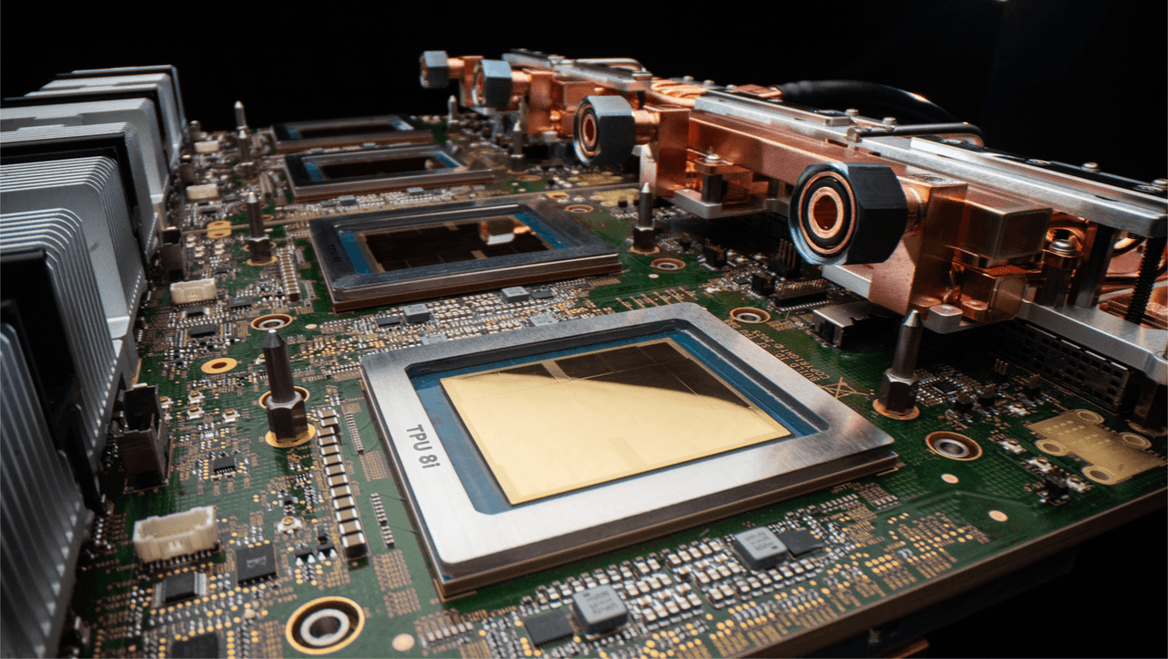
Source: Google
Efficiency gains target goodpute and power consumption
Google emphasizes a "goodpute" rate of 97 percent for TPU 8t, meaning the chips spend more time actively advancing AI model training rather than waiting or handling faults
1
. Mark Lohmeyer, Google's vice president of compute and AI infrastructure, explained that at frontier training scale, every percentage point can translate into days of active training time3
. The eighth-gen chips offer twice the performance per watt compared to Ironwood, with TPU 8t delivering 124% more performance per watt and TPU 8i providing a 117% gain4
. Google Cloud has also developed a Managed Lustre storage system capable of delivering 10 TB/s of aggregate data directly into accelerator memory3
. Data centers co-designed with TPUs feature integrated networking on a single chip and more efficient pod layouts, reportedly increasing computing power per unit of electricity by six times1
.TPU 8i optimizes inference for agent workloads
The TPU 8i for inference addresses the ongoing usage of models after users submit prompts, a workload fundamentally different from training
2
. Google tripled the on-chip SRAM to 384 MB per chip, matching Nvidia's approach with its upcoming Groq 3 LPU hardware5
. This larger cache allows TPU 8i to keep more key-value information on-chip, speeding up models with longer context windows1
. Inference pods now contain 1,152 chips versus just 256 for Ironwood inference clusters, delivering 11.6 EFlops per pod1
. The architecture is designed "to deliver the massive throughput and low latency needed to concurrently run millions of agents cost-effectively," according to Alphabet CEO Sundar Pichai5
. Lohmeyer noted that "the number of transactions is going way up, and the cost per transaction needs to go way down for it to scale" .Related Stories
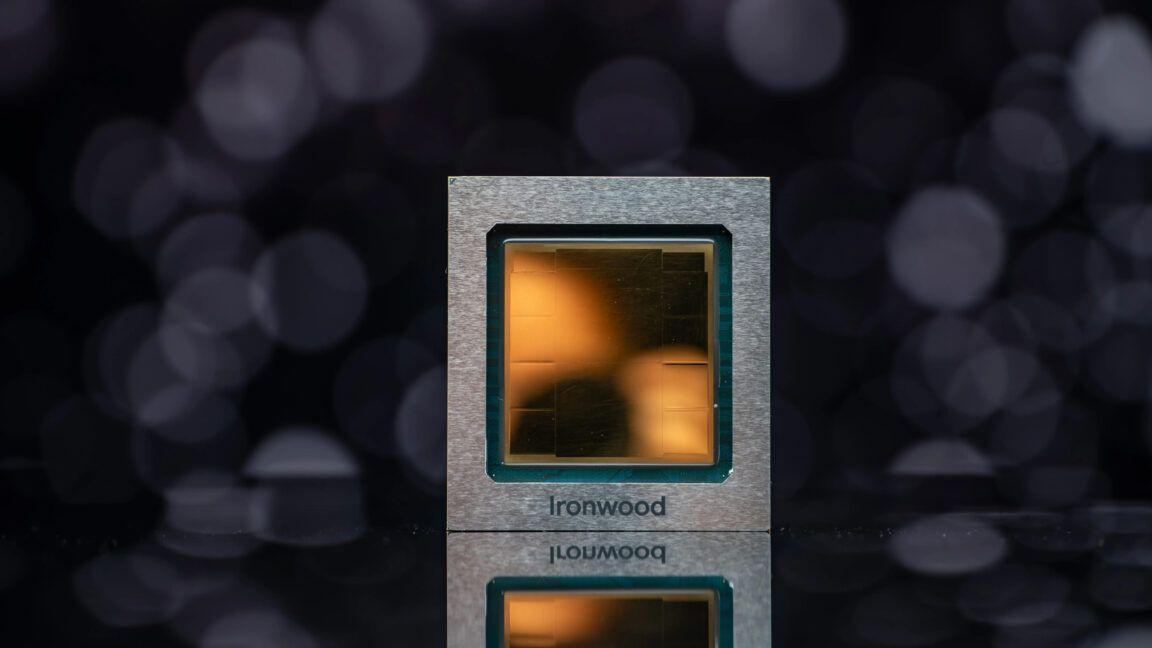
Axion CPUs replace x86 in full-stack ARM approach
The eighth-gen AI accelerators mark the first from Google to rely solely on its custom Axion ARM CPU host, featuring one CPU for every two TPUs compared to Ironwood's ratio of one x86 CPU servicing four TPU chips
1
. This "full-stack" ARM-based approach allows for greater efficiency, following a similar path to Amazon's integration of Graviton and Trainium 3 earlier this year3
. Google has also adapted its fourth-gen liquid cooling setup to the new chips, using actively controlled valves to adjust water flow based on workload1
. Both new TPUs support frameworks developers already use, including JAX, MaxText, PyTorch, SGLang, and vLLM1
.Market positioning against Nvidia and hyperscalers
Google is not replacing Nvidia entirely, continuing to offer services based on Nvidia chips and promising to deploy the upcoming Vera Rubin chip later this year
2
. The company announced collaboration with Nvidia to engineer computer networking that allows Nvidia-based systems to perform more efficiently in its cloud infrastructure, particularly enhancing the software-based networking tech called Falcon2
. Nvidia's stock price briefly dropped about 1.5 percent after Google's announcement1
. DA Davidson analysts estimated in September that the Google TPU business, coupled with Google DeepMind, would be worth about $900 billion5
. Adoption is ramping up, with Citadel Securities building quantitative research software on TPUs, all 17 U.S. Energy Department national laboratories using AI co-scientist software built on the chips, and Anthropic committing to using multiple gigawatts worth of Google TPUs5
. Both chips will power Google's Gemini-based agents and become generally available later this year1
.Source: Benzinga
References
Summarized by
Navi
[1]
[3]
Related Stories
Google Unleashes Ironwood TPU v7: Seventh-Generation AI Chips Challenge Nvidia's Dominance
06 Nov 2025•Technology
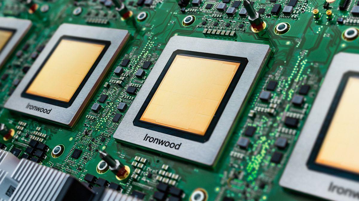
Google deploys billions to turn TPU chips into serious challenge against Nvidia's AI dominance
22 Jun 2026•Business and Economy

Google Cloud bets big on AI agents with Gemini Enterprise platform and new chips
22 Apr 2026•Technology

Recent Highlights
1
OpenAI releases GPT-5.6 models after government review, unveils ChatGPT Work to compete in AI agent race
Technology

2
Over 200 economists warn AI economic impact could eclipse Industrial Revolution in years, not decades
Policy and Regulation
3
Apple sues OpenAI for allegedly stealing trade secrets as hardware rivalry intensifies
Business and Economy
Recent Highlights
Today's Top Stories


Don’t drown in AI news. We cut through the noise - filtering, ranking and summarizing the most important AI news, breakthroughs and research daily. Follow topics that matter to you and stay ahead.


