AI Boom Turns Chip Packaging Into Critical Battleground as Companies Invest Billions


3 Sources
[1]
AI boom turns chip packaging into the next battleground for semiconductors
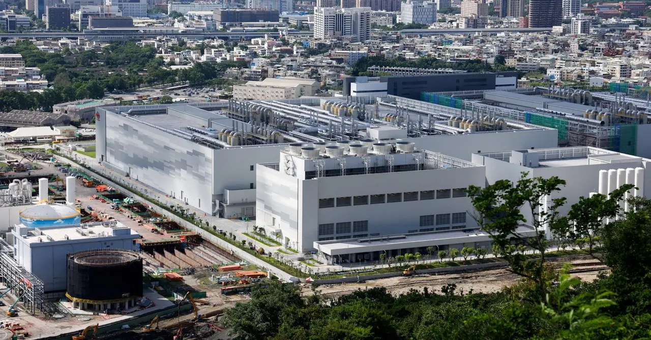
TAIPEI, Nov 6 (Reuters) - A global race to build AI infrastructure is unleashing billions of dollars of investment in advanced chip packaging, a once unglamorous aspect of technology that has become a critical bottleneck in turning out the world's most powerful processors. As demand for artificial
[2]
AI boom turns chip packaging into the next battleground for semiconductors
Billions of dollars are being invested in advanced chip packaging due to the demand for AI chips. This growing need is pushing companies to expand their production capacities significantly. Taiwan's TSMC is at the forefront of packaging technology, yet limitations have spurred alternatives. TAIPEI
[3]
AI boom turns chip packaging into the next battleground for semiconductors
TAIPEI, Nov 6 (Reuters) - A global race to build AI infrastructure is unleashing billions of dollars of investment in advanced chip packaging, a once unglamorous aspect of technology that has become a critical bottleneck in turning out the world's most powerful processors. As demand for artificial
Share
Copy Link
The global race to build AI infrastructure has transformed advanced chip packaging from an overlooked process into a critical bottleneck. With demand for AI chips outstripping capacity, companies like Nvidia and AMD are investing billions to expand production, while TSMC's dominance faces challenges from emerging alternatives.
Advanced Chip Packaging Emerges as Critical Bottleneck for AI Infrastructure
The AI boom has transformed chip packaging from a mundane manufacturing step into a strategic battleground for semiconductors
1
. As demand for artificial intelligence chips surges beyond available packaging capacity, major players from Nvidia and AMD to lesser-known Taiwanese firms are racing to expand production capabilities. Former Intel CEO Pat Gelsinger, now a partner at Playground Global, captured the shift succinctly: "Packaging was always that thing that you just didn't worry about"2
. That perception has fundamentally changed as advanced chip packaging could eventually account for as much as half the value of a chip product, with modern graphics and central processing units integrating 10 or more chips, sometimes reaching 201
.Market Dynamics Point to Massive Investment Wave
Research firm Yole Group forecasts that revenue from advanced packaging will overtake traditional methods for the first time in 2026, with capital spending on the technology expected to near $28 billion
2
. This represents a fundamental change in chipmaking as the industry confronts bottlenecks for high-performance AI processors. The surge in investment reflects how critical this once-unglamorous aspect of semiconductor manufacturing has become to turning out the world's most powerful processors. Interviews with more than a dozen industry executives and analysts reveal equipment makers are developing new tools specifically to address capacity constraints3
.TSMC Dominates but Faces Capacity Limits
Taiwan's TSMC, the world's largest contract chipmaker, dominates the most sophisticated advanced packaging technology, including chip-on-wafer-on-substrate, or CoWoS
1
. This technology links separate pieces of silicon—processors and memory chips—on a shared base to enable high-speed collaboration. CoWoS is widely deployed by Nvidia, AMD, and Broadcom, as well as cloud companies developing their own AI chips2
. However, TSMC's capacity limits have created urgent pressure on chip designers to seek additional supply sources. The global race to expand advanced chip packaging capacity has opened opportunities for smaller suppliers eager to capture market share.Nvidia Funds Billions to Expand Alternative Capacity
Nvidia is providing billions of dollars in financing to expand CoWoS packaging capacity at Siliconware Precision Industries, or SPIL, a unit of Taiwan's ASE Technology, according to an industry executive familiar with the matter
1
. The funding will support new factory space and equipment, with the scale of this support not previously reported. Neither Nvidia nor ASE Technology commented on the arrangement, but the move signals how seriously chip designers view the capacity crunch. This investment underscores the strategic importance of securing packaging capacity to meet surging demand for AI chips and avoid production delays.Why Advanced Packaging Matters for AI Performance
The scramble to invest reflects a broader fundamental change in chipmaking. More chip designers now use advanced packaging to integrate multiple chips—processors and memory—into a single package
3
. This approach allows components to work together faster as one system, contrasting sharply with decades of practice when packaging mainly protected chips and provided electrical connections to circuit boards. The shift has accelerated as winning performance gains by shrinking and adding transistors becomes harder and costlier. Advanced packaging techniques prove especially vital for AI chips, which must shuffle vast amounts of data between processors and nearby memory. Speeding up such transfers through faster data processing directly accelerates training and running AI models2
.Related Stories
Powertech Technology Bets on Panel-Level Innovation
TSMC's tight capacity offers opportunities for smaller suppliers like Taiwan's Powertech Technology. Chairman D K Tsai told reporters in August: "Everyone is looking for a solution outside TSMC. They don't want to rely entirely on TSMC"
1
. Powertech, also known as PTI, is betting heavily on panel-level packaging, which uses larger rectangular panels instead of round wafers as the chip packaging platform. This innovation accommodates more chips in each production run and wastes less material—critical advantages as AI processors grow larger and more complex. PTI is collaborating with AMD and Broadcom to demonstrate the technology's viability for larger, more complex chip packages used in AI and high-performance computing3
.Major Investments Signal Long-Term Commitment
Powertech plans to invest $400 million in an advanced packaging joint venture with Broadcom in Singapore, with production potentially beginning in 2028
2
. PTI Senior Vice President Jim Lin emphasized that "the most important thing right now is capacity," noting customers are waiting for the company to ramp up production. Meanwhile, AMD has unveiled investments exceeding $10 billion across Taiwan's semiconductor industry, including partnerships with ASE Technology, SPIL, and Powertech Technology on advanced packaging1
. TSMC itself is developing panel-based technology called chip-on-panel-on-substrate, or CoPoS, to support larger and more complex chip packages. The company built a pilot line in April and expects production to begin within a couple of years, though CoWoS remains its main AI-packaging technology3
. These investments position the industry to meet escalating demands from the AI boom while diversifying supply chains beyond single-source dependencies.References
Summarized by

Navi
[3]
Related Stories
Intel bets billions on advanced packaging as Google and Amazon eye alternatives to TSMC bottleneck
06 Apr 2026•Technology

TSMC Advances Chip Packaging Technology to Boost AI Performance by 2027
16 Apr 2025•Technology
Intel Emerges as Alternative to TSMC's Strained CoWoS Packaging as AI Demand Surges
25 Nov 2025•Business and Economy
Recent Highlights



Recent Highlights
Today's Top Stories










Don’t drown in AI news. We cut through the noise - filtering, ranking and summarizing the most important AI news, breakthroughs and research daily. Follow topics that matter to you and stay ahead.


