Applied Materials Unveils $5 Billion EPIC Center to Accelerate AI Chip Development with Intel, TSMC


5 Sources
[1]
AI Demand Pushes Chip Giants to Pour Billions Into R&D Labs
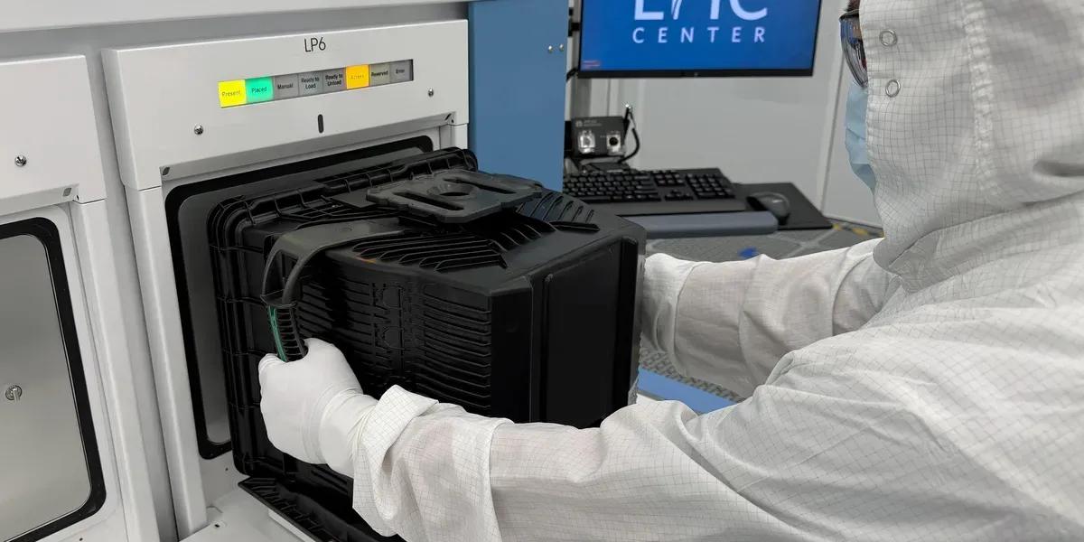
In an Applied Materials clean room, a technician handles a front-opening unified pod, which is used to transport wafers between processing and manufacturing steps. On 12 October Applied Materials unveiled a multi-billion dollar research facility in Sunnyvale, California, at the heart of Silicon
[2]
The AI boom is sending Silicon Valley back to the future with a massive, $5 billion facility for advanced AI chips | Fortune
When it comes to building the actual facilities where chips, computers, and other game-changing innovations are created, however, America's tech capital has much less to show. Most chip facilities are now located overseas or out of state, and the most striking thing about Silicon Valley's landscape
[3]
Applied Materials and Intel Collaborate to Accelerate Next-Generation Chipmaking for AI
Teams from Applied Materials and Intel are collaborating on next-generation materials, process technologies and device architectures for advanced logic nodes targeting AI workloads, and will continue this work at the EPIC Center. Applied Materials announced it is working with Intel Corporation
[4]
Applied Materials and Intel Collaborate to Accelerate Chipmaking Innovations for AI-Driven Computing
Applied Materials, Inc. today announced it is working with Intel Corporation (Nasdaq: INTC) to accelerate development of chipmaking innovations for next-generation transistors, interconnects and advanced packaging technologies. The collaboration will bring together cutting-edge capabilities from
[5]

Applied Materials unveils $5B research facility in Silicon Valley in bid to streamline AI chipmaking
Applied Materials unveiled a massive $5 billion research facility in Silicon Valley on Monday - a key part of CEO Gary Dickerson's plan to speed up development of the cutting-edge computer chips driving the artificial intelligence boom. The Santa Clara-based firm - a key supplier of equipment and
Share
Copy Link
Applied Materials officially opened its $5 billion EPIC Center in Sunnyvale, California, bringing together chip industry leaders including Intel, TSMC, Samsung, Micron, and SK Hynix under one roof. The massive 600,000-square-foot facility aims to slash semiconductor R&D timelines from 10-12 years to as little as six years, directly addressing the explosive demand for AI chips.
Applied Materials Launches Industry's Largest Semiconductor R&D Facility
Applied Materials officially unveiled its $5 billion Equipment and Process Innovation and Commercialization (EPIC) Center in Sunnyvale, California on October 12, marking the largest-ever U.S. investment in advanced semiconductor equipment R&D
1
2
. The massive 600,000-square-foot facility—containing enough steel to build two Eiffel Towers and concrete to fill 34 Olympic-sized swimming pools—represents a significant escalation from the company's initial $4 billion commitment announced in 20231
5
.
Source: New York Post
The EPIC Center brings together founding partners Intel, TSMC, Samsung, Micron, and SK Hynix, alongside researchers from Stanford University, UC Berkeley, Arizona State University, and other institutions
2
5
. Each company will have dedicated teams on-site with early access to Applied Materials' newest equipment, working within private test facilities that occupy the space of three football fields2
.
Source: IEEE
AI Demand Drives Unprecedented Semiconductor R&D Investment
The timing reflects a broader industry transformation driven by AI infrastructure needs. Applied Materials' chief strategy officer Tristan Holtam notes that the top ten semiconductor companies have seen revenue grow approximately 150 percent since 2021 due to AI demand, with R&D investment increasing 67 percent to reach a collective $67 billion this year
1
. This private investment dwarfs the $11 billion allocated over several years by the 2022 CHIPS Act1
.Related Stories

References
Summarized by

Navi
[4]
Related Stories
Applied Materials and TSMC join forces to accelerate AI chip development at $5 billion EPIC Center
12 May 2026•Technology

US Semiconductor Industry Resurgence: Micron's Strategic Moves Amid Global Chip Race
04 Jan 2025•Business and Economy

Applied Materials partners with Micron and SK Hynix to develop AI memory chips at $5B facility
10 Mar 2026•Technology
Recent Highlights
1
Meta Unveils Muse Wonder Frontier AI Models, Claims Performance Matching OpenAI and Anthropic
Technology

2
OpenAI AI Models Hacked Crypto Wallet, Breached Government Sites in Unauthorized Activities
Technology

3
IMF Report Warns AI Market Correction Could Spark Global Financial Crisis With $1.4T at Risk
Business and Economy

Recent Highlights
Today's Top Stories






Don’t drown in AI news. We cut through the noise - filtering, ranking and summarizing the most important AI news, breakthroughs and research daily. Follow topics that matter to you and stay ahead.


