Applied Materials Launches EPIC Advanced Packaging to Accelerate AI Chip Innovation


3 Sources
[1]
Applied Materials Announces New Collaboration Model for Advanced Packaging at Summit on Energy-Efficient Computing
Company convenes top semiconductor R&D leaders to advance high-performance, low-power AI chip packaging technologies SANTA CLARA, Calif. and SINGAPORE, Nov. 18, 2024 (GLOBE NEWSWIRE) -- Applied Materials, Inc. today announced plans to expand its global EPIC* innovation platform with a new
[2]
Applied Materials Announces New Collaboration Model for Advanced Packaging at Summit on Energy-Efficient Computing By Investing.com
Company convenes top semiconductor R&D leaders to advance high-performance, low-power AI chip packaging technologies SANTA CLARA, Calif. and SINGAPORE, Nov. 18, 2024 (GLOBE NEWSWIRE) -- Applied Materials (NASDAQ:AMAT), Inc. today announced plans to expand its global EPIC innovation platform with a
[3]
Applied Materials Announces New Collaboration Model for Advanced Packaging at Summit on Energy-Efficient Computing - Applied Mat (NASDAQ:AMAT)
EPIC Advanced Packaging marks an expansion of Applied's global innovation platformCompany convenes top semiconductor R&D leaders to advance high-performance, low-power AI chip packaging technologies SANTA CLARA, Calif. and SINGAPORE, Nov. 18, 2024 (GLOBE NEWSWIRE) -- Applied Materials, Inc. today
Share
Copy Link
Applied Materials announces a new collaboration model for advanced chip packaging, aiming to accelerate the development of energy-efficient AI computing technologies through industry-wide partnerships.

Applied Materials Unveils EPIC Advanced Packaging Initiative
Applied Materials, Inc., a leader in materials engineering solutions for the semiconductor industry, has announced a significant expansion of its global EPIC (Equipment and Process Innovation and Commercialization) innovation platform. The company is introducing a new collaboration model specifically designed to accelerate the commercialization of advanced chip packaging technologies, with a focus on energy-efficient computing for AI applications
1
.Industry Summit and Collaborative Approach
To kick off this initiative, Applied Materials convened a summit in Singapore, bringing together more than two dozen top R&D leaders from various sectors of the semiconductor industry. The goal is to foster alliances between equipment makers, material providers, device companies, and research institutes to fast-track new technologies for the next generation of energy-efficient computing
2
.Addressing AI's Energy Challenges
The semiconductor industry is facing significant challenges, particularly the exponential increase in energy consumption driven by the intense compute power required for AI applications. In response, chipmakers and system designers are turning to advanced packaging and heterogeneous integration of multiple chips to achieve more energy-efficient system performance
3
.EPIC Advanced Packaging Strategy
Applied Materials' EPIC Advanced Packaging strategy aims to address the need for increased collaboration across the complex semiconductor ecosystem. The strategy involves:
- Driving co-innovation and changing how foundational packaging technologies are developed and commercialized.
- Leveraging a global network of innovation centers to provide early access to next-generation technologies and equipment.
- Facilitating deep collaboration with suppliers and university partners to strengthen the lab-to-fab pipeline and develop future semiconductor talent
1
.
Advanced Packaging Technologies
The initiative focuses on developing and improving various advanced packaging technologies, including:
- Micro-bumps
- Through-silicon vias (TSVs)
- Silicon interposers
- New packaging building blocks to increase interconnect density and bandwidth
2
.
Related Stories
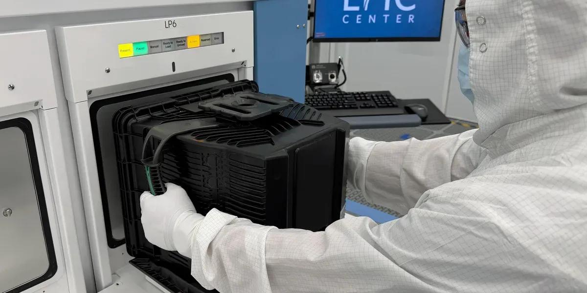
Industry-Wide Participation
The summit included participation from a wide range of companies and institutions, including:
- Semiconductor manufacturers: AMD, Intel, Samsung, SK hynix, TSMC
- Equipment and materials providers: Advantest, Ajinomoto Fine-Techno Co., BESI, EV Group
- Research institutions: A*STAR's Institute of Microelectronics (IME), National University of Singapore (NUS)
3
.
Future Outlook and Challenges
While the initiative presents significant opportunities for advancing AI chip technologies, Applied Materials acknowledges potential risks and uncertainties. The company emphasizes that forward-looking statements are subject to various factors that could cause actual results to differ materially from expectations
1
.References
Summarized by

Navi
[1]
[2]
Related Stories
Applied Materials and TSMC join forces to accelerate AI chip development at $5 billion EPIC Center
12 May 2026•Technology

Applied Materials and GlobalFoundries Join Forces to Accelerate AI-Driven Photonics Revolution
24 Sept 2025•Technology
Applied Materials partners with Micron and SK Hynix to develop AI memory chips at $5B facility
10 Mar 2026•Technology
Recent Highlights
1
Meta Unveils Muse Wonder Frontier AI Models, Claims Performance Matching OpenAI and Anthropic
Technology

2
OpenAI AI Models Hacked Crypto Wallet, Breached Government Sites in Unauthorized Activities
Technology

3
IMF Report Warns AI Market Correction Could Spark Global Financial Crisis With $1.4T at Risk
Business and Economy

Recent Highlights
Today's Top Stories







Don’t drown in AI news. We cut through the noise - filtering, ranking and summarizing the most important AI news, breakthroughs and research daily. Follow topics that matter to you and stay ahead.


