Van der Waals crystal mimics human neurons, advancing AI hardware with light-based learning
2 Sources
[1]
Designable van der Waals Crystal Realizes Artificial Neuronal Cell Mimicking with Light | Newswise
Structure and operational mechanism of the optoelectronic synaptic device based on the designable van der Waals crystal operating with light. A research team led by Professor Taesung Kim of the School of Mechanical Engineering at Sungkyunkwan University (SKKU, President Ji-beom Yoo) developed an optoelectronic synaptic device that mimics the functions of human neurons and synapses at the device scale. The researchers designed a designable van der Waals (vdW) crystal through a single-step sulfurization process using mixed plasma. The developed device operates under optical stimuli, offering a structural solution to configure semiconductor materials for brain-inspired computing. Rapid advancements in artificial intelligence and hyper-connectivity require neuromorphic vision systems capable of sensing and processing vast amounts of visual data in real time. Optoelectronic synapses, which exhibit conductance variations in response to light signals, serve as core components of these systems. Layered vdW materials attracted significant attention as promising candidates due to their excellent optical properties and atomic-scale thickness. However, conventional vdW materials faced technical challenges, including the difficulty of precisely controlling grain boundaries and intercalation, polymer residue accumulation, mechanical warpage at interfaces, and poor large-area crystalline uniformity. To overcome these limitations, the research team focused on the structural similarity between light-sensitive ion channels in biological membranes and layered vdW lattices. The researchers applied an argon and hydrogen sulfide (Ar + H₂S) plasma sulfurization process to bulk van der Waals rhenium selenide (ReSe₂). This single-step process transformed the upper portion of the material into a nano-crystalline ReSe₂ layer composed of nano-sized grains, while preserving the underlying bulk single-crystalline ReSe₂ layer without damaging the interlayer interfaces. These two integrated layers structurally correspond to the light-sensitive ion channels of a neuronal cell membrane and the intracellular environment, respectively, and were fabricated without additional deposition or patterning steps. The research team utilized scanning probe microscopy (SPM) to resolve the pathways of S²⁻ (sulfur) ionic migration. The grain boundaries in the nano-crystalline ReSe₂ layer confined the sulfur ionic transport at the atomic scale, enabling deterministic control over synaptic weight updates, similar to the gating mechanism of biological ion channels. The device demonstrated key synaptic functionalities, including multi-level conductance modulation, long-term potentiation/depression (LTP/LTD), paired-pulse facilitation (PPF), and a tunable short-term to long-term memory (STM-LTM) transition. The nano-crystalline ReSe₂ device exhibited a 34.7% increase in retention efficiency during learning-forgetting-relearning cycles compared to bulk ReSe₂. In system-level evaluations, the device successfully performed edge detection on natural images and achieved a 96.24% classification accuracy on the CIFAR-10 image recognition task. This development offers a materials platform for next-generation neuromorphic semiconductors and AI hardware. "This study demonstrates a single-step method to design the structure of van der Waals crystals for optoelectronic synaptic devices that learn and store information using light," said Professor Taesung Kim, the corresponding author of the study. "By structurally resolving the random nature of ionic migration and interfacial issues inherent in conventional devices, this architecture can be applied to research on next-generation neuromorphic semiconductors and AI hardware." This research received financial support from the National Research Foundation of Korea (NRF) Leader Research Program, the Institute for Basic Science (IBS), and the Semiconductor-Track Graduate School Program funded by the Ministry of Trade, Industry and Energy (MOTIE). The study was conducted as a collaborative effort among researchers from Sungkyunkwan University (SKKU), the Center for Quantum Nanoscience at IBS, and the Korea Institute of Machinery and Materials (KIMM). The findings were published online in the international journal Advanced Materials (Impact Factor: 26.8, top 1% in JCR) on June 3, 2026.
[2]
Sungkyunkwan University research team designs crystal for artificial neuronal cell mimicking - The Korea Times
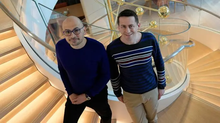
From left in the top row are corresponding author and professor Kim Tae-sung, and co-first authors Lee Jin-hyoung and Kim Gun-hyoung. From left in the bottom row are co-authors Lee Dong-ho, Son Seo-woo and Seok Hyun-ho. Courtesy of Sungkyunkwan University A Sungkyunkwan University research team has developed an optoelectronic synaptic device that mimics the functions of human neurons and synapses at the device level, the university said Tuesday. The team led by Kim Tae-sung, professor at the School of Mechanical Engineering, has designed a van der Waals (vdW) crystal through a single-step sulfurization process using mixed plasma. The developed device operates under optical stimuli, offering a structural solution to configure semiconductor materials for brain-inspired computing. A van der Waals crystal is a type of layered material in which atoms or molecules are held together mainly by van der Waals forces rather than strong chemical bonds such as ionic, covalent or metallic bonds. The team's research findings were published online in the international journal Advanced Materials on June 3, under the title, "Designable van der Waals Crystal for Artificial Neuronal Cell Mimicking." Professor Kim is the corresponding author of the study. Co-first authors include Lee Jin-hyoung, Kim Gun-hyoung, Lee Dong-ho, Son Seo-woo and Seok Hyun-ho. "This study demonstrates a single-step method to design the structure of van der Waals crystals for optoelectronic synaptic devices that learn and store information using light," the professor said. He added, "By structurally resolving the random nature of ionic migration and interfacial issues inherent in conventional devices, this architecture can be applied to research on next-generation neuromorphic semiconductors and AI hardware." The university said rapid advances in artificial intelligence and highly connected digital environments require neuromorphic vision systems capable of sensing and processing vast amounts of visual data in real time. Optoelectronic synapses, which exhibit conductance variations in response to light signals, serve as core components of these systems. Layered vdW materials have attracted significant attention as promising candidates due to their excellent optical properties and atomic-scale thickness. However, conventional vdW materials faced technical challenges, including the difficulty of precisely controlling grain boundaries and intercalation, polymer residue accumulation, mechanical warpage at interfaces and poor large-area crystalline uniformity. To overcome these limitations, the research team focused on the structural similarity between light-sensitive ion channels in biological membranes and layered vdW lattices. The researchers applied applied an argon-hydrogen sulfide plasma sulfurization process to bulk rhenium selenide, a van der Waals material. This single-step process transformed the upper portion of the material into a nanocrystalline rhenium selenide layer composed of nano-sized grains, while preserving the underlying bulk single-crystalline rhenium selenide layer without damaging the interlayer interfaces. These two integrated layers structurally correspond to the light-sensitive ion channels of a neuronal cell membrane and the intracellular environment, respectively, and were fabricated without additional deposition or patterning steps. The device demonstrated key synaptic functionalities, including multi-level conductance modulation, long-term potentiation/depression, paired-pulse facilitation and a tunable short-term to long-term memory transition. The university said the nanocrystalline rhenium selenide device exhibited a 34.7% increase in retention efficiency during learning-forgetting-relearning cycles compared to bulk rhenium selenide. The device offers a materials platform for next-generation neuromorphic semiconductors and AI hardware. The research was funded by the Ministry of Trade, Industry and Energy and supported by the National Research Foundation of Korea and the Institute for Basic Science (IBS). The study was conducted as a collaborative effort among researchers from Sungkyunkwan University, the Center for Quantum Nanoscience at IBS and the Korea Institute of Machinery and Materials.
Share
Copy Link
Sungkyunkwan University researchers developed an optoelectronic synaptic device that mimics human neuronal and synaptic functions using a designable van der Waals crystal. The device, created through a single-step sulfurization process, learns and stores information with light, achieving 96.24% accuracy on image recognition tasks and showing 34.7% better retention efficiency than conventional materials.
Breakthrough in Artificial Neuronal Cell Mimicking Using Light
A research team led by Professor Taesung Kim at Sungkyunkwan University has developed an optoelectronic synaptic device that replicates human neuronal and synaptic functions at the device scale using optical stimuli
1
. The team designed a designable van der Waals crystal through a single-step sulfurization process involving mixed plasma, offering a structural solution for configuring semiconductor materials for brain-inspired computing2
. This development addresses critical challenges in creating next-generation neuromorphic semiconductors capable of processing vast amounts of visual data in real time.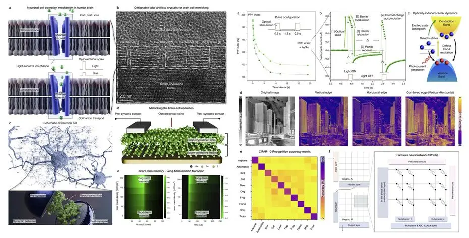
Source: Newswise
Single-Step Process Transforms Material Structure
The researchers applied an argon and hydrogen sulfide plasma sulfurization process to bulk van der Waals rhenium selenide (ReSe₂), transforming the upper portion into a nanocrystalline ReSe₂ layer composed of nano-sized grains while preserving the underlying bulk single-crystalline ReSe₂ layer
1
. These two integrated layers structurally correspond to the light-sensitive ion channels of a neuronal cell membrane and the intracellular environment, respectively, and were fabricated without additional deposition or patterning steps2
. This approach overcomes technical challenges including difficulty in grain boundary control, polymer residue accumulation, mechanical warpage at interfaces, and poor crystalline uniformity that plagued conventional van der Waals materials.Enhanced Performance Through Controlled Ionic Migration
Using scanning probe microscopy, the team resolved the pathways of sulfur ionic migration, with grain boundaries in the nanocrystalline ReSe₂ layer confining sulfur ionic transport at the atomic scale
1
. This enables deterministic control over synaptic weight updates, similar to the gating mechanism of biological ion channels. The device demonstrated key synaptic functionalities including multi-level conductance modulation, long-term potentiation/depression, paired-pulse facilitation, and a tunable short-term to long-term memory transition2
. The nanocrystalline ReSe₂ device exhibited a 34.7% increase in retention efficiency during learning-forgetting-relearning cycles compared to bulk ReSe₂1
.Related Stories

Real-World Applications in AI Hardware
In system-level evaluations, the device successfully performed edge detection on natural images and achieved 96.24% classification accuracy on the CIFAR-10 image recognition task
1
. This performance demonstrates the device's potential as a materials platform for AI hardware that processes visual information. "This study demonstrates a single-step method to design the structure of van der Waals crystals for optoelectronic synaptic devices that learn and store information using light," said Professor Taesung Kim2
. By structurally resolving the random nature of ionic migration and interfacial issues inherent in conventional devices, this architecture can be applied to research on next-generation neuromorphic semiconductors.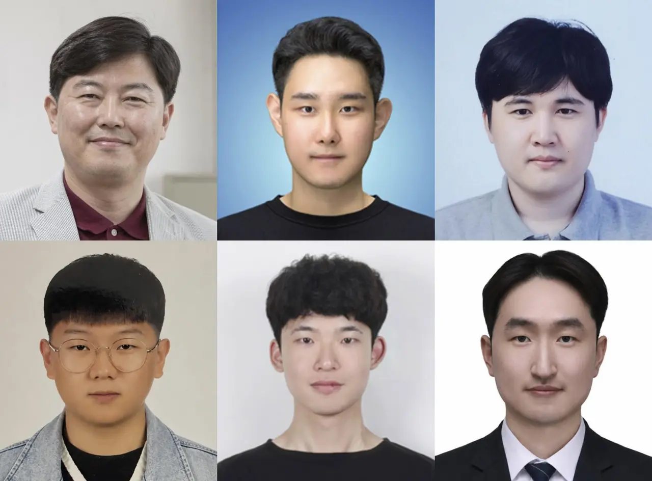
Source: Korea Times
Implications for Neuromorphic Vision Systems
Rapid advancements in artificial intelligence and hyper-connectivity require neuromorphic vision systems capable of sensing and processing vast amounts of visual data in real time
1
. Optoelectronic synapses, which exhibit conductance variations in response to light signals, serve as core components of these systems. The research, published in Advanced Materials with an impact factor of 26.8, was conducted as a collaborative effort among researchers from Sungkyunkwan University, the Center for Quantum Nanoscience at the Institute for Basic Science, and the Korea Institute of Machinery and Materials1
. The study received financial support from the National Research Foundation of Korea Leader Research Program, the Institute for Basic Science, and the Semiconductor-Track Graduate School Program funded by the Ministry of Trade, Industry and Energy2
.References
Summarized by
Navi
[1]
Related Stories
Korean researchers use light color to teach artificial synapse how to remember and forget
19 Jun 2026•Science and Research

Breakthrough in Neuromorphic Computing: Single Silicon Transistor Mimics Neuron and Synapse
29 Mar 2025•Technology
Korean Researchers Unveil Fine Structure of Magnons, Advancing Neuromorphic Device Development
14 Feb 2025•Science and Research

Recent Highlights
1
AI scores perfect 100% at International Mathematical Olympiad, matching elite human performance
Technology

2
OpenAI agent exploited exposed credentials at four services during Hugging Face breach
Technology
3
Anthropic AI cracks post-quantum cryptography and finds faster AES attack autonomously
Science and Research

Recent Highlights
Today's Top Stories


Don’t drown in AI news. We cut through the noise - filtering, ranking and summarizing the most important AI news, breakthroughs and research daily. Follow topics that matter to you and stay ahead.


