Fujitsu Monaka CPU Stacks Entire Cache on Separate 5nm Die, Delivers 2x AI Performance


2 Sources
[1]
Hot Chips 2026: Fujitsu's Monaka CPU stacks its entire cache on a separate 5nm die and narrows to 256-bit SVE2
This Tom's Hardware Premium article is free to read with a Tom's Hardware account; no payment necessary. We're offering free access from August 23 to 26 so you can read all of our reporting from Hot Chips. Fujitsu gave us a detailed look at its 144-core Monaka server CPU at Hot Chips 2026 on
[2]
Fujitsu's Monaka Chip 3D Stacks 2nm "144-Core CPU" With 5nm "SRAM" Dies While Monaka-X Eyes 2029 Release on 1.4nm & NVLink Fusion
Fujitsu's Monaka CPU launches in 2027 with 144 cores, 2.9 GHz, 500W TDP, & 2x AI performance using Arm v9.3-A architecture and 3D chiplets. Fujitsu's Monaka Stacks a 2nm 144-Core CPU Atop 5nm SRAM Dies, Cutting Silicon Area 30% for 2027 Launch Fujitsu is preparing the upcoming Monaka CPU, which
Share
Copy Link
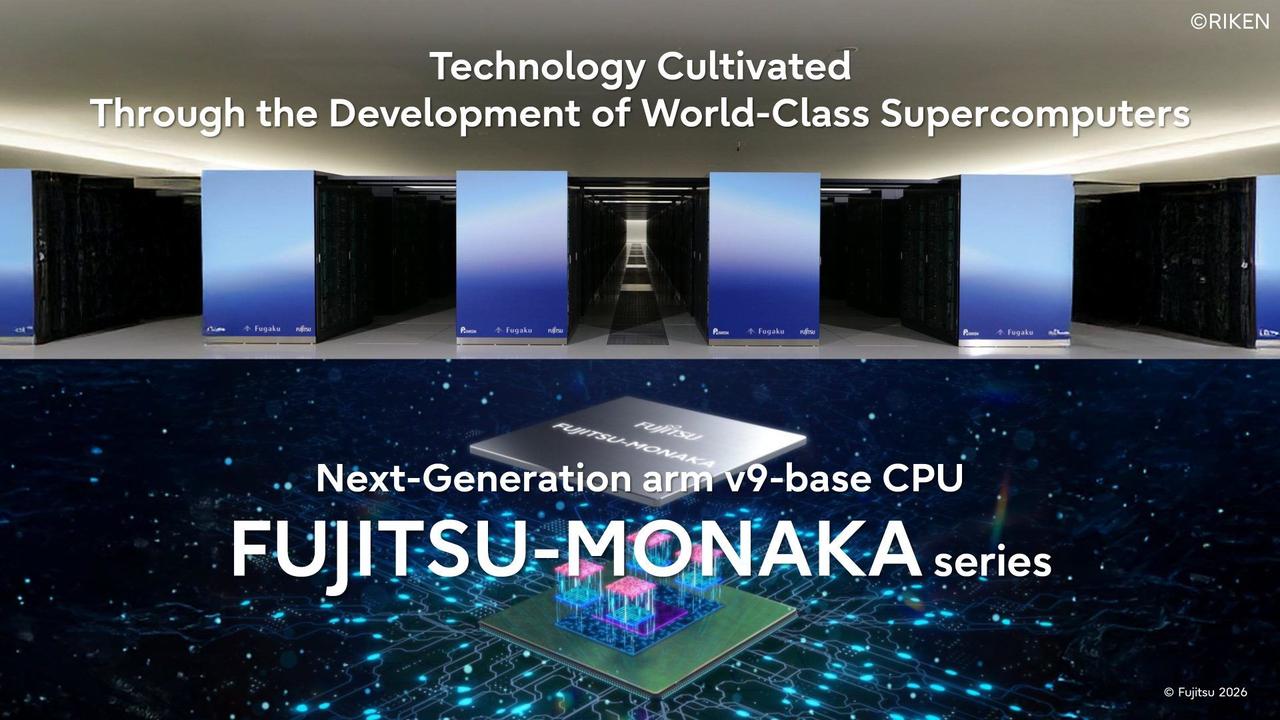
Fujitsu unveiled its 144-core Monaka server CPU at Hot Chips 2026, featuring a 2nm compute die stacked atop a 5nm SRAM die that holds the entire last-level cache. The chip targets green AI data centers with dual 256-bit SVE2 vector units, 12-channel DDR5-8000 memory, and ships in 350W and 500W SKUs for 2027 production.
Fujitsu Monaka CPU Debuts Three-Die Stack Architecture at Hot Chips 2026
Fujitsu presented its 144-core Monaka server CPU at Hot Chips 2026 on August 24, revealing a three-tier silicon design that places the entire last-level cache on a separate 5nm SRAM die beneath a 2nm compute die
1
2
. Ryohei Okazaki, lead architect of Fujitsu's processor development team, positioned the chip as "a made-in-Japan CPU, specifically engineered for AI performance and power efficiency" for green AI data centers, subsidized by Japan's New Energy and Industrial Technology Development Organization1
. The Fujitsu Monaka CPU ships in two SKUs: a 350W air-cooled variant running at 2.1 GHz base frequency and a 500W liquid-cooled part at 2.9 GHz base, with evaluation samples available now and volume production scheduled for 20271
.
Source: Wccftech
2nm Core Die and 5nm SRAM Die Reduce Silicon Area by 30%
The 144-core processor splits into three distinct silicon tiers: a 2nm core die on TSMC N2P, a 5nm SRAM die on TSMC N5 housing the complete last-level cache, and a 5nm IO die
1
2
. The core die stacks face-to-face on top of the 5nm SRAM die through hybrid bonding, positioned on the cooling side because it runs hottest, while the IO die connects to the SRAM die across a silicon interposer1
. Fujitsu keeps 2nm silicon under 30% of total die area, a strategy Okazaki said lets the company "accelerate the time to market for our 2-nanometer-based chip" by pushing components that shrink poorly onto the 5nm dies1
. Each core measures approximately 1.47mm²1
2
. The chiplet-based disaggregated architecture allows Fujitsu to select the most suitable technology for each design component, optimizing for power efficiency, performance, and cost2
.256-bit SVE2 Vector Units Replace 512-bit SVE for Data Center Efficiency
The Fujitsu Monaka CPU runs dual 256-bit SVE2 vector units per core, down from the 512-bit SVE in its A64FX predecessor that powered the Fugaku supercomputer
1
. When Chester Lam of Chips and Cheese asked why Fujitsu narrowed the vector datapath, Okazaki explained the chip is built "for [the] data center" and that the company wanted to "minimize the core size" for optimal cost and performance, with narrower units also cutting SIMD width for general-purpose code1
. The Arm v9.3-A architecture core carries two 256-bit-wide execution units aligned to two 256-bit load/store units, with FP8 and INT8 matrix support added for AI inference workloads1
2
. Monaka drops HBM for 12-channel DDR5 memory at 8000 MT/s and includes 96 PCIe 6.0 lanes with CXL 3.0 support1
2
.AI Performance Targets 96.2 TOPS with Ultra-Low-Voltage Operation
Fujitsu estimates the 500W high-performance SKU delivers 6,013 GFLOPS in DGEMM and 96.2 TOPS in INT8, while the 350W high-efficiency SKU achieves 4,355 GFLOPS and 69.7 TOPS, with both variants rated around 500 GB/s in STREAM Triad
1
2
. The company claims up to 2x AI performance and over 50% TCO reduction against unnamed comparisons, crediting ultra-low-voltage operation that runs the core around 30% below nominal voltage for roughly half the power1
2
. Okazaki described the voltage technique as delivering "energy saving comparable to moving one generation beyond the 2 nanometers," achieved with custom SRAM and a proprietary CAD flow tuned for non-standard low-voltage operation1
. Low-dropout voltage regulators sit on the 5nm SRAM die directly beneath the core's floating-point units to enable per-core dynamic voltage and frequency scaling1
2
.Related Stories

Mainframe-Class Reliability and Flexible NUMA Node Configuration
The server CPU carries mainframe-class reliability features inherited from Fujitsu's processor line: ECC or duplication on the L1 and L2 caches, parity checks on execution units and registers, and a hardware instruction-retry mechanism to recover from transient errors
1
2
. The core runs a three-level TAGE branch predictor and six ALUs for general-purpose throughput1
. Monaka supports flexible NUMA node methodology for memory access, configurable into 18 core x 8 NUMA node for last-level cache latency/throughput optimization, 36 core x 4 NUMA node for memory latency/throughput balancing, or 144 cores x 1 NUMA node for large-size memory applications2
. The platform supports two sockets per node, delivering 288 cores total, and includes confidential computing capabilities for secure in-use data protection2
.Monaka Enters Competitive Arm Server Market in 2027
By 2027, the 144-core Monaka will land in the middle of the Arm server field rather than at the top. AWS's Graviton5 reaches 192 Neoverse V3 cores on a single 3nm die, Ampere's roadmap runs to 512 cores in AmpereOne Aurora, and Microsoft's Cobalt 200 packs 132 cores with its own per-core DVFS
1
. Monaka's differentiation rests on the cache-on-die stack and 12-channel DDR5 bandwidth rather than core count, and its 256-bit SVE2 width matches SiPearl's Rhea1 while exceeding the 128-bit SVE2 common to hyperscaler Arm cores1
. When Dr. Ian Cutress of More Than Moore asked whether Fujitsu was "doing anything special to minimize core-to-core latency" given that core dies sit on opposite sides of the package and traffic routes through the IO die, Fujitsu pointed to the face-to-face hybrid bonding between the core and SRAM dies but declined to disclose latency figures1
. Fujitsu is already sampling the chip, with production shipments commencing in 2027, and planning a Monaka-X successor targeting 2029 release with NVLink Fusion support2
.References
Summarized by

Navi
[1]
Related Stories
Fujitsu and Supermicro Join Forces to Develop Green AI Computing Solutions
03 Oct 2024•Technology

AMD unveils Helios rack-scale AI system with 72 MI455X accelerators and 256-core EPYC Venice
06 Jan 2026•Technology

Fujitsu and Rapidus partner to build 1.4nm AI chip entirely in Japan with government backing
31 Mar 2026•Technology
Recent Highlights
1
Meta Unveils Muse Wonder Frontier AI Models, Claims Performance Matching OpenAI and Anthropic
Technology

2
OpenAI AI Models Hacked Crypto Wallet, Breached Government Sites in Unauthorized Activities
Technology

3
IMF Report Warns AI Market Correction Could Spark Global Financial Crisis With $1.4T at Risk
Business and Economy

Recent Highlights
Today's Top Stories








Don’t drown in AI news. We cut through the noise - filtering, ranking and summarizing the most important AI news, breakthroughs and research daily. Follow topics that matter to you and stay ahead.


