Microsoft-backed Lace Lithography raises $40M to create chip designs 10 times smaller


3 Sources
[1]
Chip lithography start-up Lace raises $40m for tech development
The funds could enable significant advances in semiconductor design and manufacturing. Lace Lithography, a Microsoft-backed Norwegian chipmaking equipment start-up, has announced the raising of $40m to be used in the advancement of its unique semiconductor technologies. The Series A funding round
[2]
Microsoft-Backed Lace Raises $40M for Helium Beam Lithography
Microsoft-backed chipmaking equipment startup Lace has secured $40 million in funding. This investment aims to advance technology that will significantly enhance semiconductor design and manufacturing. On March 23, 2026, the Norway-based AI startup announced its new goal of revitalizing the chip
[3]
Microsoft-backed startup raises $40 million for advanced chipmaking equipment tech
SAN FRANCISCO, March 23 (Reuters) - Lace, a Norway-headquartered chipmaking equipment startup which is backed by Microsoft, has raised $40 million in funding to further develop a technology that could enable significant advances in semiconductor design and manufacturing, the company said on
Share
Copy Link
Norway-based Lace Lithography has secured $40 million in Series A funding to develop helium atom beam lithography technology. The Microsoft-backed startup aims to create chip designs 10 times smaller than what's currently possible, potentially transforming semiconductor manufacturing with atomic resolution capabilities by 2029.
Microsoft-Backed Startup Secures $40M to Transform Semiconductor Manufacturing
Lace Lithography, a Norwegian startup backed by Microsoft, announced it has raised $40 million in Series A funding to advance its groundbreaking helium atom beam lithography technology
1
. The round was led by Atomico, with additional investments from M12, Microsoft's venture arm, along with Linse Capital, the Spanish Society for Technological Transformation, and Nysnø3
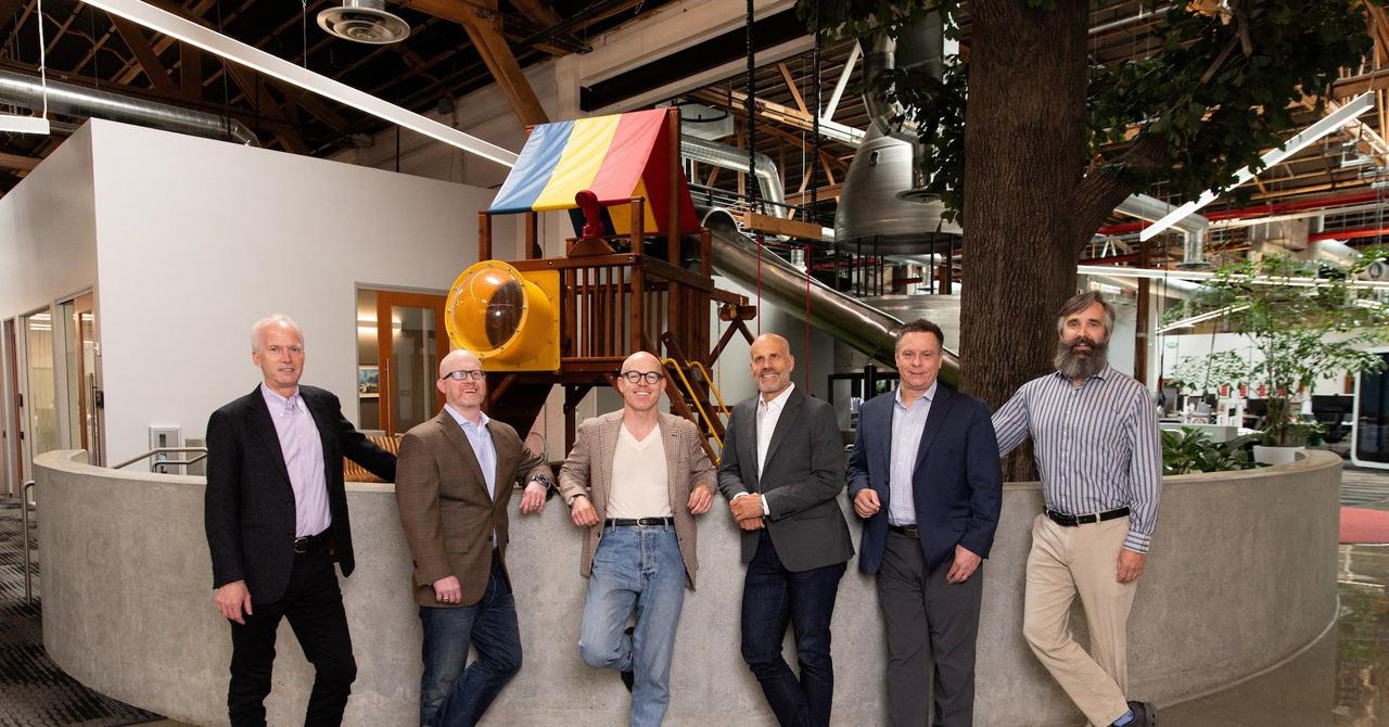
. Founded in 2023 by CEO Bodil Holst and Adrià Salvador Palau, the company is headquartered in Bergen, Norway, with a second location in Barcelona, Spain.
Source: Analytics Insight
Novel Lithography System Challenges ASML's Dominance
Traditionally, manufacturers like Intel and Taiwan Semiconductor Manufacturing Company use light-based lithography systems made by Dutch company ASML to create the complex circuits that form the foundation of artificial intelligence chips
2
. ASML currently dominates the market for advanced chipmaking equipment as manufacturers race to shrink chip components and squeeze more features into limited silicon areas. However, Lace Lithography has developed an entirely different approach that could reshape the semiconductor landscape. Instead of using light, the company's engineers created a novel lithography system that utilizes a helium atom beam to etch circuits onto silicon wafers1
.
Source: Silicon Republic
Chip Designs 10 Times Smaller Than Current Capabilities
The breakthrough technology enables chip designs 10 times smaller than what is currently possible, according to Bodil Holst
3
. The beam Lace will use to make chips is about the width of a single hydrogen atom, or 0.1 nanometer, compared to ASML's lithography tools that use a beam of light measuring approximately 13.5 nanometers3
. For context, a human hair is about 100,000 nanometers wide. John Petersen, Scientific Director of Lithography at Imec, a research and innovation hub for the chip industry, explained that the main advantage of the helium atom beam is the ability to create features such as transistors to an "almost unimaginable" degree of miniaturization3
.Related Stories

Atomic Resolution Could Unlock Next-Generation AI Processors
Holst stated that Lace's advancements could allow chipmakers to print silicon wafers at what she described as "ultimately atomic resolution"
1
. This capability would give manufacturers the ability to ramp up the performance of AI processors well beyond current capabilities when manufacturing advanced chips. "Our technology is a way that can potentially expand the roadmap and be an enabler for doing things that would not have been possible otherwise," Holst told Reuters3
. Smaller transistors and other features created through systems integration would directly impact the computing horsepower achievable on limited silicon areas, crucial for the development of next-generation artificial intelligence chips.Timeline Points to 2029 for Pilot Chip Fabrication Plant
Lace Lithography has already developed prototype systems and presented its findings in an invited research paper at a scientific lithography summit in February
3
. The company aims to have a test tool operational in a pilot chip fabrication plant by approximately 20291
. While the company declined to comment on its overall valuation, the $40m funding represents significant investor confidence in a field that has drawn fresh interest from investors and governments as a new round of startups emerges, some aiming to compete directly with established players in photonics packaging and semiconductor manufacturing3
.References
Summarized by

Navi
[1]
[2]
Related Stories
Silicon Valley Startup xLight Raises $40 Million to Develop Advanced Chip-Making Laser Technology
22 Jul 2025•Technology
Dutch Chip Manufacturing Startup Nearfield Instruments Secures €135M in Funding
19 Jul 2024

Lumilens Exits Stealth at $5.5B Valuation to Fix AI Data Centers' Connectivity Crisis
06 Aug 2026•Startups
Recent Highlights
1
OpenAI AI Models Hacked Crypto Wallet, Breached Government Sites in Unauthorized Activities
Technology

2
IMF Report Warns AI Market Correction Could Spark Global Financial Crisis With $1.4T at Risk
Business and Economy

3
Amazon Bee Unveils Two Personal AI Devices Starting at $75 with Real-Time Conversation Tracking
Technology
Recent Highlights
Today's Top Stories









Don’t drown in AI news. We cut through the noise - filtering, ranking and summarizing the most important AI news, breakthroughs and research daily. Follow topics that matter to you and stay ahead.


