4 Sources
[1]
Tensordyne's Wild Log Math Aims to Leave Nvidia's AI Chips In the Dust
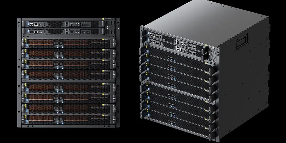
Tensordyne's Napier pods fit 72 of its new AI chips in a system that takes up one-quarter of a server rack. If simulations are to be believed, startup Tensordyne's new AI chip could crush the performance of market leader Nvidia in terms of energy efficiency and latency for inferencing. The company just sent the plans for its first chip to be manufactured, with commercial sales of a 72-chip system scheduled for the second half of 2027. Tensordyne claims its 72-chip system can run large LLMs four times as fast using one-fifth the power compared to a 72-Nvidia GB300 system. However, real systems won't be around to back these figures up until the end of the year. The not-so-secret sauce behind the outsized efficiency of Tensordyne's new chip, Napier, is how it does matrix multiplication, the main math of AI. It takes advantage of the fact that the logarithm of A times B equals the logarithm of A plus the logarithm of B. "We've turned multipliers into adders," explains Gilles Backhus, a Tensordyne founder and vice president of AI. Adders are smaller and more energy efficient logic circuits than those that do multiplication, he says. So Napier can pack more compute into a smaller area and still save on power. New kinds of numbers That such a thing was possible has long been known, but there wasn't a good way to use it, because converting back and forth between logarithmic numbers and the floating point numbers that describe neural networks took too much time and energy and introduced too many inaccuracies. Not anymore, according to Backhus. "So far no one has figured out how to do the linear to logarithm and logarithm to linear conversion as we have," he says. "And that's actually the crux of that whole thing. Our engineers have figured out ways to do this very elegantly and very very accurately and cheaply on silicon." The importance of number formats hasn't been lost on the AI industry. Speaking at IEEE Hot Chips in 2023, Nvidia chief scientist attributed the majority of the improvement in the company's GPUs at the time to the use of shorter number formats and the smaller circuits they require. Researchers have also worked on circuits to compute with alternative formats, such as the logarithm-like posit and more recently its scientific-computing counterpart the takum. However, these formats have not reached mainstream adoption mostly because their hardware implementation is so different from traditional floating point. Inference Demands Influence Architecture Market trends, including the rise of AI agents, mean inference -- the execution of neural network models -- is becoming more important than training new large-language models. Factors like the cost and the speed at which answers are delivered are starting to dominate, and that's led AI companies to look for system architectures that are a better fit for that. Tensordyne executives say they saw this coming and engineered their computers to meet it. There are two main parts to executing an LLM: prefill and decode. In the prefill stage the model takes in the input text and turns it into tokens, the basic units it can work with, and builds a kind of working memory about the input, called the key value cache. It's a computationally heavy task. Decode is where the LLM generates its output tokens, the answer or response to your input. Each new token is predicted using the previous token and the key-value cache. This sequential nature can make decode a slower process, and it's more dependent on memory and network latency than computing power. So, AI chip makers are starting to build systems with those two different demands in mind. Nvidia is touting a system where a server rack full of B300 GPUs handles prefill and several racks of its Groq 3 processors do the decode. Amazon Web Services is combining a rack of its Trainium AI chips for prefill with several racks of Cerbras's wafer-scale computers for decode. Tensordyne says its system can handle both jobs. "We're optimizing for two hard challenges here at the same time," says R.K. Anand, chief product officer and co-founder of Tensordyne. "We're the first company proving that you can do both without going to multiple vendors and multiple racks." The dense compute needed for prefill comes from the logarithmic math. The needs of decode come from 144-gigabytes of high-bandwidth memory and a custom 1-microsecond-latency network called Tensordyne Napier Link. In a "pod" system that fits in one quarter of a standard rack, Tensordyne packs in 72 Napier chips, 8 Intel Xeon CPUs, and 64 terabytes of solid-state storage. A 4-pod rack working on a 2-trillion parameter LLM would deliver 1300 tokens per second per user at a cost of $11 for 1 million tokens while consuming 120 kilowatts of power, the company claims, with one pod crunching out prefill and 3 working on decode. To get similar tokens per second per user numbers a 9-rack Rubin and Groq 3 system would likely consume 1.5 megawatts, according to Tensordyne. Whether or not these numbers really hold up will have to wait until later in the year. Tensordyne plans to have a beta version available through the cloud for customers to work with. It expects to begin shipping systems to customers about a year from now.
[2]
Tensordyne makes a big bet on log math to beat Nvidia
AI infrastructure startup Tensordyne has taped out its first commercial accelerator, with fabrication on TSMC's 3nm process already underway. Developed in collaboration with Juniper Networks and Broadcom, Tensordyne's systems promise higher throughput and lower power consumption than GPUs. It claims to achieve this using an unorthodox approach to mathematics that uses logarithms -- which you might recall from high school arithmetic -- to make matrix multiplication heavy AI workloads less computationally intensive to run. In conventional computing, addition is cheap, multiplication is expensive. Logarithms flip this on its head. Using logs, multiplication essentially becomes an additional problem. a*b becomes log(a) + log(b). The trick is converting those values to logs and back again efficiently. There are a couple of ways of dealing with this. One of the easier options would have been to use a look up table (LUT). However, Tensordyne cofounder Gilles Backhus tells El Reg that relying on LUTs would have been too large to be practical. Instead, the company uses a heuristic, specifically the Mitchell approximation, to estimate log and antilog for each value. This is still an approximation and on its own introduces too much error to be tenable. To overcome this, Backhus tells us Tensordyne has implemented a section-wise correction mechanism in hardware that delivers accuracy equivalent to that of FP16. However, it's worth noting that Napier will also support FP8 and 4-bit block floating datatypes. In effect, Tensordyne claims to have built a chip in which the multiply accumulate (MAC) unit works without actually doing multiplication in the conventional sense. The result is a chip that delivers power efficiency significantly greater than what you'd see on modern GPUs. Or at least that's the claim. Tensordyne says its rack systems will spit out up to 17x more tokens per watt and achieve 13x higher throughput than Nvidia's Blackwell systems. Dissecting Napier Tensordyne's first commercial chip, Napier, boasts many of the same specs you'd have seen from a high-end GPU just a couple years ago. The accelerator boasts a 300-watt nominal TDP, 144 GB of HBM3e spread across four stacks, 4.7 TB/s of memory bandwidth, and up to 2.1 petaFLOPS of dense FP8 performance. This makes it roughly comparable to Nvidia's H200 accelerators announced in 2023 while using nearly 60 percent less power. Having said that, max achieved FLOPS often fall far short of peak FLOPS, so take that comparison with a grain of salt. We won't know how Napier actually compares to Nvidia or AMD's latest generation of GPUs until it arrives next year. Backhus tells us that Tensordyne is leaning heavily on the scalability of its accelerators rather than individual performance. Each chip features roughly a terabyte of interconnect bandwidth allowing for rack scale deployments of up to 72 accelerators per pod. The TDN72 Tensordyne's system, codenamed the TDN72, consists of eight air-cooled compute blades each with a single 10-core Intel Xeon-D host CPU and nine Napier accelerators. These chips are interconnected by a high-speed interconnect fabric topology reminiscent of the one used by Nvidia's GB200 NVL72 rack systems. Each chip connects to six proprietary fabric switch blades developed by Tensordyne's networking partner Juniper, located at the back of the system, in an all-to-all fabric. Despite some similarities to Nvidia's NVL72 racks, Tensordyne's TDN72 will be much much smaller and won't require liquid cooling, which should make it easier to deploy in older brownfield datacenters. According to Backhus, up to four 30kW TDN72 systems can be packed into an -- admittedly large -- 52U rack. That works out to 608 petaFLOPS in a 120kW footprint, or about 1.68x more dense FP8 compute per rack than Nvidia's GB200 NVL72. That doesn't take into consideration the fact that Nvidia's kit supports NVFP4 acceleration while Napier is limited to FP4 weights. But again, don't read too much into that comparison. Peak FLOPS are not representative of real world performance. Tensordyne's TDN72 launches next year, and it'll be competing against Nvidia's next-gen Vera Rubin and Vera Rubin Ultra systems, which will no doubt be a stiffer fight, especially when software compatibility is taken into consideration. Software promises Since building its first prototype silicon a few years ago, the company has gone to great lengths to keep its software platform as simple, and easy for customers to deploy, as possible. For example, the prototype lacked the error correction found in its Napier chips, and would have required users to use quantization-aware training to adapt their models to run accurately on the hardware -- not exactly feasible for those looking to run trillion-parameter models. The software has also matured such that the hardware's compiler can convert existing models to run directly on its latest hardware, an approach we've seen from other chip startups like Tenstorrent. For inference, Tensordyne has developed its own proprietary serving platform, as well as a runtime environment that Backhus says will allow customers to use their preferred inference servers, such as vLLM. PyTorch support is under development. Before the chip has even shipped, the company is making some bold performance claims. Backhus expects the chips to deliver upwards of 1,000 tokens a second, and that's without relying on multi-token prediction or other forms of speculative decoding to boost token generation. Tensordyne's platform has certainly attracted the attention of neocloud providers like Cirrascale and BlueSky Compute, both of which have expressed interest in deploying the company's hardware when available. But, as we've seen with AMD and others, software can make or break a chipmaker. With Napier slated for release in Q2 or Q3 of 2027, Tensordyne won't have long to get things right. ®
[3]
US AI startup Tensordyne claims 3nm Napier chip outperforms NVIDIA Blackwell by 13x in tokens per second
A US-based AI startup is making bold claims against NVIDIA's most advanced hardware. Tensordyne has announced the successful tape-out of its Napier chip, a 3nm AI accelerator built on TSMC's process in collaboration with Broadcom and HPE's Juniper Networks. The company is already reporting over $200 million in projected system demand. The Napier chip packs 138 billion transistors, 2.1 petaflops of Dense FP8 compute, 144GB of HBM3E memory, 256MB of SRAM, and runs at 300W TDP. The architectural hook is a proprietary logarithmic mathematics method that replaces numerous multiplication operations with simpler addition-based computation. Because adders are smaller and more power-efficient than multipliers, Tensordyne claims this frees up significantly more silicon area for SRAM, which it says gives Napier five times as much on-chip SRAM as NVIDIA's Blackwell. The full rack configuration, called the TDN72, houses 288 Napier chips across four pods of 72 chips each. The complete rack delivers 608 petaflops of FP8 compute, 42TB of HBM3E memory, and operates within a 120kW power envelope, all while being fully air-cooled. Tensordyne claims the TDN72 provides 13x more tokens per second and 17x more tokens per watt than NVIDIA's Blackwell NVL72, and says a single rack can match the throughput of nine NVIDIA Rubin plus Groq LPX racks for multi-trillion parameter models. The company also points to a proprietary scale-up interconnect called TDN Link, which it says delivers sub-microsecond chip-to-chip latency with 1TB/s of bandwidth across the 72-chip system, targeting mixture-of-experts and agentic AI workloads where interconnect performance matters as much as raw compute. Those are impressive numbers, but they come with the standard caveats that apply to any pre-launch AI accelerator. Tensordyne's beta program is planned for Q1 2027, with broader system shipments expected by the end of Q2 2027. By that point, NVIDIA, AMD, and a growing field of inference-focused silicon startups will have moved on as well. Tensordyne promises compatibility with Hugging Face-hosted models and PyTorch, and with Triton, and provides a custom Python SDK. If Tensordyne's technology works and can be delivered in 2027, Napier could be a notable alternative for inference infrastructure.
[4]
Tensordyne's 3nm Napier AI Chip Promises 13x Higher Token Throughput Than Blackwell & Blazes Past Rubin With 1000 Tokens/s In Multi-Trillion Parameter Models
US-based AI company, Tensordyne, has announced the successful tape-out of its Napier chip, which it claims to demolish NVIDIA's Blackwell & Rubin chips with leading token throughput and efficiency. Tensordyne's new Napier AI Chip arrives with one clear mission: to make NVIDIA's Blackwell and Rubin chips look considerably less impressive The Napier chip will be the core component of the Tensordyne Napier TDN system, which is designed in collaboration with Broadcom and HPE Juniper Networks. The Napier platform has one goal: to unify AI through novel logarithmic AI math, a tightly integrated memory architecture, and a high-performance scale-up interconnect that drives higher token throughput at low power. Napier is built on TSMC's 3nm process, and with its successful tape-out, the chip is now in production. With the primary milestone achievement, Tensordyne is now working towards beta deployment and a broader infrastructure plan that represents over $200 million in forecasted Napier system demand. And the key area of focus is AI inferencing. We just talked about how current AI infrastructure is constrained by power consumption, but to tackle these constraints, solutions such as 800V DC are going to incur a huge deployment cost. Infrastructures such as power and cooling alone make up 50% of the cost of major AI deployments, and to address these, Tensordyne has come up with a new inference stack across math, compute, memory, and networking: TDN Math (Logarithmic Mathematics) TDN replaces large-scale multiplication operations with simplified addition-based computation, significantly improving performance-per-watt efficiency across frontier AI models. TDN AIP (Artificial Intelligence Processor) Each TDN processor tightly integrates substantial fast SRAM alongside HBM memory, minimizing idle compute cycles and supporting efficient execution of the industry's largest models. TDN Link (Any-to-Any Scale-Up Interconnect) Tensordyne's proprietary scale-up fabric delivers sub-microsecond communication latency between processors, maximizing compute utilization and minimizing interconnect bottlenecks. All of this is brought together in Tensordyne's TDN72 Inference Pod and Rack system. Each Pod is fitted with 72 Napier AI chips, which are composed of NVIDIA's NVL72 rack with 72 Blackwell or Rubin GPUs. It requires way less infrastructure capacity, and a Napier Rack combines for TDN72 pods to deliver: * 17x more tokens per watt (vs NVIDIA Blackwell) * 13x more tokens per second (vs NVIDIA Blackwell) * Up to $33 million more annual revenue per rack Tensordyne doesn't stop at just Blackwell comparison; they also compare the Napier solution against NVIDIA's upcoming Rubin platform. The company claims that its platform supports multi-trillion parameter models with a throughput of 1000 tokens/s per use in a single-rack configuration. To do the same, NVIDIA will require nine Rubin + Groq LPX racks. Tensordyne's Napier platform represents a bold leap forward in AI inference. By delivering 17× more tokens per watt and 13× higher throughput than NVIDIA Blackwell, while matching the performance of nine Rubin-based racks in a single compact footprint, it shatters the traditional speed-versus-cost and power-versus-performance trade-offs. With dramatically lower infrastructure demands, up to $33 million more annual revenue per rack, and efficient scaling for multi-trillion parameter models, Napier doesn't just compete with NVIDIA's Blackwell & Rubin; it redefines what's possible for next-generation AI deployment. Follow Wccftech on Google to get more of our news coverage in your feeds.
Share
Copy Link
AI chip startup Tensordyne has completed tape-out of its Napier AI chip, built on TSMC's 3nm process. The company claims its logarithmic matrix multiplication approach delivers 13x more tokens per second and 17x better tokens per watt than Nvidia Blackwell systems. With over $200 million in projected demand, Tensordyne plans beta deployment in Q1 2027 and broader shipments by mid-2027.
AI chip startup Tensordyne has announced the successful tape-out of its Napier AI chip, marking a significant milestone in its quest to outperform Nvidia Blackwell in AI inference workloads
1
. Built on TSMC's 3nm process in collaboration with Broadcom and HPE's Juniper Networks, the chip is now in production with beta deployment scheduled for Q1 2027 and commercial shipments expected by the end of Q2 20272
. The company has already secured over $200 million in projected system demand, signaling strong early interest in its unconventional approach to AI acceleration3
.
Source: The Register
What sets Tensordyne apart is its use of logarithmic matrix multiplication, a mathematical technique that transforms multiplication operations into simpler addition problems. By leveraging the principle that the logarithm of A times B equals the logarithm of A plus the logarithm of B, the company has effectively turned multipliers into adders. "We've turned multipliers into adders," explains Gilles Backhus, Tensordyne founder and vice president of AI
1
. Since adders are smaller and more power-efficient than multiplication circuits, this approach allows Napier to pack significantly more compute into a smaller silicon area while consuming less power.The concept of using logarithms for computation isn't new, but previous attempts failed because converting between logarithmic numbers and the floating-point numbers used in neural networks introduced too much latency, energy overhead, and accuracy loss. Tensordyne claims to have solved this fundamental challenge. "So far no one has figured out how to do the linear to logarithm and logarithm to linear conversion as we have," Backhus states
1
. The company uses the Mitchell approximation as a heuristic to estimate log and antilog values, combined with a section-wise correction mechanism implemented in hardware that delivers accuracy equivalent to FP162
. This elegant solution avoids the impracticality of look-up tables while maintaining the precision required for large language models.The Napier AI chip itself packs 138 billion transistors and delivers 2.1 petaflops of dense FP8 compute performance
3
. Each chip features 144GB of HBM3E memory spread across four stacks, providing 4.7TB/s of memory bandwidth, along with 256MB of SRAM—five times more on-chip SRAM than Nvidia's Blackwell4
. Operating at a 300-watt TDP, Napier uses nearly 60 percent less power than Nvidia's H200 accelerators while delivering comparable specifications2
. The chip also supports FP8 and 4-bit block floating datatypes, providing flexibility for different model requirements.
Source: IEEE
Tensordyne's full rack configuration, the TDN72 system, houses 288 Napier chips across four pods of 72 chips each
3
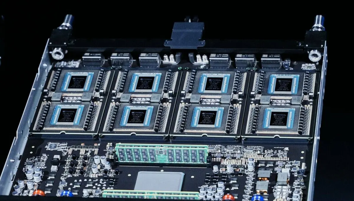
. Each pod consists of eight air-cooled compute blades, with each blade containing a single 10-core Intel Xeon-D host CPU and nine Napier accelerators2
. The complete rack delivers 608 petaflops of FP8 compute and 42TB of HBM3E memory while operating within a 120-kilowatt power envelope—all without requiring liquid cooling3
.The chips connect through a proprietary interconnect called TDN Link, which delivers sub-microsecond chip-to-chip latency with 1TB/s of bandwidth across the 72-chip system
3
. Each chip connects to six proprietary fabric switch blades developed by Juniper Networks in an all-to-all fabric topology reminiscent of Nvidia's GB200 NVL72 rack systems2
. Despite similarities, the TDN72 is significantly more compact—up to four 30kW systems can fit into a 52U rack, making deployment in older brownfield datacenters more feasible.Related Stories
As AI inference workloads become more critical than training, particularly with the rise of AI agents, companies are optimizing for the two main stages of executing large language models: prefill and decode. Prefill is computationally intensive, converting input text into tokens and building the key-value cache. Decode generates output tokens sequentially, making it more dependent on memory and network latency than raw compute power
1
. While Nvidia is touting split architectures—B300 GPUs for prefill and Groq 3 processors for decode—Tensordyne claims its system can handle both jobs efficiently. "We're optimizing for two hard challenges here at the same time," says R.K. Anand, chief product officer and co-founder of Tensordyne. "We're the first company proving that you can do both without going to multiple vendors and multiple racks"1
.For a 2-trillion parameter model, Tensordyne claims a 4-pod rack would deliver 1,300 tokens per second per user at a cost of $11 per million tokens while consuming 120 kilowatts of power
1
. The company asserts the TDN72 provides 13x more tokens per second and 17x more tokens per watt than Nvidia's Blackwell NVL724
. For multi-trillion parameter models, Tensordyne claims a single rack can match the throughput of nine Nvidia Vera Rubin plus Groq LPX racks, delivering 1,000 tokens per second per user4
. These performance claims translate to up to $33 million more annual revenue per rack compared to competing solutions4
.Tensordyne has worked to simplify software deployment since building its first prototype silicon. Early prototypes lacked error correction and required quantization-aware training, making them impractical for trillion-parameter models
2
. The current platform promises compatibility with Hugging Face-hosted models, PyTorch, and Triton, along with a custom Python SDK that can convert existing models to run directly on the hardware3
.However, the standard caveats apply. These performance figures come from simulations, and real systems won't be available until late 2027 to verify the claims
1
. By the time Tensordyne ships, it will compete against Nvidia's next-generation Vera Rubin and Vera Rubin Ultra systems, presenting a stiffer challenge, especially regarding software compatibility2
. The 3nm AI accelerator landscape will also feature competition from AMD and a growing field of inference-focused silicon startups3
. For organizations deploying AI infrastructure, power efficiency and cost-per-token metrics will determine whether Tensordyne's logarithmic approach can disrupt Nvidia's dominance in a market where software ecosystems often matter as much as raw performance.Summarized by
Navi
[2]
[3]
27 May 2026•Technology

03 Jan 2026•Technology

12 Feb 2026•Technology

1
Policy and Regulation

2
Policy and Regulation

3
Policy and Regulation