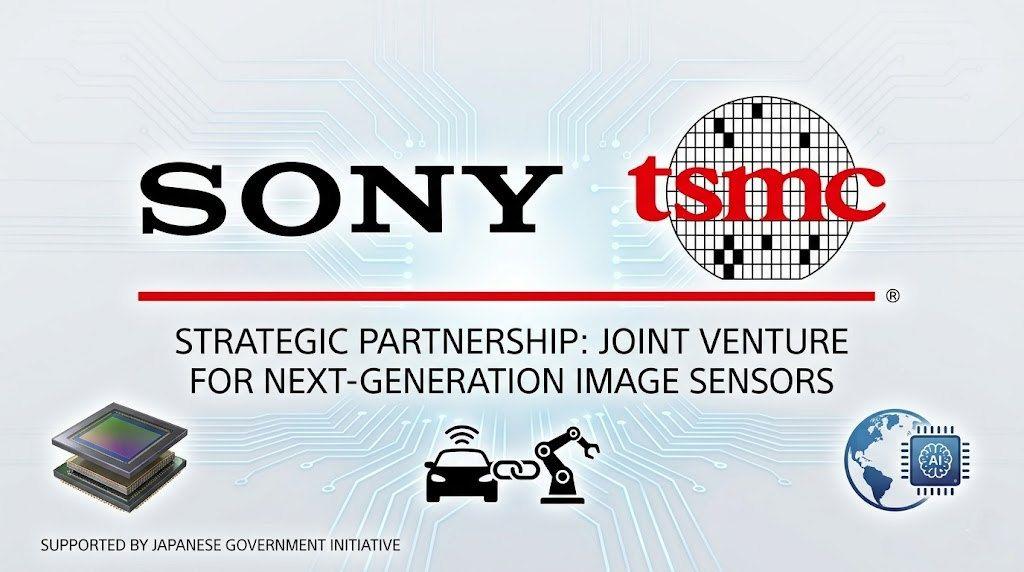
Sony and TSMC form joint venture to build next-generation image sensors for AI and robotics
4 Sources
[1]
Sony, TSMC form Japanese joint venture to push image sensors into automotive and robotics
TSMC and Sony Semiconductor Solutions have signed a non-binding memorandum of understanding to establish a joint venture (JV) for next-generation image sensor development and manufacturing, with Sony holding the majority and controlling interest. The JV will be sited at Sony's newly constructed fab in Koshi City, Kumamoto Prefecture. Sony is also planning additional capital investment at its existing Nagasaki plant. Both investment tracks are expected to be implemented in phases based on market demand and are contingent on Japanese government support. The partnership's stated scope extends beyond conventional imaging into automotive and robotics -- areas the two companies framed as emerging opportunities in physical AI applications. Sony Semiconductor Solutions President and CEO Shinji Sashida said the JV "brings together the strengths of both companies" and that Sony intends to "create new markets through unprecedented ideas and distinctive technologies," building on the partnership. TSMC Senior Vice President and Deputy Co-COO Dr. Kevin Zhang described the deal as "a key step forward in driving future sensing technology in the AI era," adding that it reflects a shared commitment to delivering leading sensing technology and products. What this signals By taking a minority stake in a Sony-controlled venture on Sony's own turf, TSMC gains a stable long-term anchor customer in image sensors while limiting capital exposure. The explicit callout of automotive and robotics is the most forward-looking element; image sensors are becoming core infrastructure for AI perception systems, and locking in next-generation process collaboration now positions both companies ahead of a potentially significant demand cycle in physical AI hardware. Japanese government support being written into the deal's premise also continues the broader trend of state-backed semiconductor capacity building across allied nations.
[2]
Sony taps TSMC as a manufacturing partner for next-gen image sensors in a new Japan-based joint venture
Sony is teaming up with chip manufacturing giant TSMC to form a joint venture to build a sensor fabrication facility in Japan for next-generation image sensors. The two companies announced a non-binding memorandum of understanding to form a strategic partnership to co-develop and co-manufacture these sensors. The proposed joint venture would have Sony as the majority and controlling shareholder, leading the project at its newly constructed fabrication facility in Koshi City, Kumamoto Prefecture, while leveraging TSMC's manufacturing expertise to produce sensors with enhanced performance compared to what is available today. The move comes as part of CEO Hiroki Totoki's plan to shift the company away from its physical assets and toward IP. That strategy has already seen Sony pull out of TV manufacturing, handing TCL a 51% stake of its Bravia division. Beyond manufacturing, the two companies are also eyeing opportunities in physical AI applications, specifically automotive and robotics, where high-performance sensing is becoming increasingly critical. Totoki told Bloomberg the move represents the "first step to becoming fab-light," an attempt by Sony to reduce its in-house manufacturing scope by bringing in partners. "Until now, we have handled everything in-house, from R&D to manufacturing, but going forward, we hope to advance manufacturing not only on our own but also by bringing in partners," he said. Sony and TSMC are now evaluating investment options before moving forward with a definitive, legally binding partnership agreement. Earlier reporting by Reuters noted that Japan's Ministry of Economy, Trade, and Industry has confirmed subsidies of up to ¥60 billion (approximately US$380 million) for Sony's Kumamoto image sensor facility. TSMC already has a presence in Kumamoto through its first fab there, which entered mass production in late 2024, supplying Sony Semiconductor Solutions and DENSO with chips built on 22/28nm and 12/16nm nodes. The new joint venture would push that relationship into more advanced territory. Sony arguably makes the gold standard image sensor right now, with the latest iPhones and much of the camera industry, including Nikon and Fujifilm, relying on its sensors. However, Samsung has been steadily gaining ground in supplying sensors for Apple, making this partnership particularly important for Sony as competition in the image sensor market intensifies.
[3]
TSMC, Sony Semiconductor Solutions to establish image sensor joint venture in Kumamoto - The Economic Times
Taiwan Semiconductor Manufacturing (TSMC) and Sony Semiconductor Solutions Corp., on Friday, announced plans to establish a joint venture in Kumamoto, Japan, to develop and produce next-generation image sensors. According to a report by Focus Taiwan, the two companies signed a non-binding memorandum of understanding (MOU) to facilitate the partnership. Under the proposed terms, Sony held a majority controlling stake in the new joint venture. The project focused on building dedicated development and production lines within Sony's newly constructed fabrication plant located in Koshi City, Kumamoto. "Sony has been our long-time partner in the CMOS (complementary metal-oxide-semiconductor) image sensor business," the report quoted TSMC Senior Vice President and Deputy Co-COO Kevin Zhang, addressing the partnership. "We are excited to elevate our collaboration to the next level, which represents a key step forward in driving future sensing technology in the AI era," Zhang added. The cooperation aimed to combine Sony's established expertise in sensor design with TSMC's advanced manufacturing capabilities and process technology. This technical synergy focused on enhancing the performance of image sensors to meet evolving industry standards. The companies also planned to explore growth opportunities in specific sectors, including robotics and automotive applications. Sony Semiconductor Solutions President and CEO Shinji Sashida expressed confidence in the joint venture and its potential impact on the industry. Sashida said he was delighted by the joint venture plan as the cooperation represented the beginning of efforts to pair up the two companies' strengths. The joint venture "aims to drive further advancement in technology and business within the next-generation image sensor field," the report quoted Sashida. TSMC said it was in discussions with Sony about potential investments by the joint venture, adding that the investments along with new capital spending by Sony in its existing plant in Nagasaki will be carried out in phases based on market demand and are expected to receive support from the Japanese government. The final establishment of the joint venture remained subject to the signing of a definitive binding agreement and the completion of customary closing conditions. Through another joint venture with Japan Advanced Semiconductor Manufacturing Inc. (JASM), TSMC currently operates an advanced wafer fab in Kumamoto, with construction of the second fab underway. Sony Semiconductor Solutions is one of the Japanese shareholders of JASM with TSMC taking a majority stake.
[4]
Sony and TSMC sign MoU for image sensor JV
Sony Semiconductor Solutions Corporation and Taiwan Semiconductor Manufacturing Company Limited (TSMC) have signed a non-binding memorandum of understanding (MOU) outlining a new strategic partnership. The agreement details plans to collaborate on the development and manufacturing of next-generation image sensors. Under the proposed terms, the two technology companies intend to establish a joint venture (JV), with Sony operating as the majority and controlling shareholder. The JV's development and production lines are slated to be housed within Sony's newly constructed fabrication facility in Koshi City, Kumamoto Prefecture. The partnership is designed to integrate the core competencies of both firms, combining Sony's background in image sensor design with TSMC's established process technology and manufacturing infrastructure. Following the signing of the MOU, Sony and TSMC are currently in discussions regarding the financial framework of the joint venture. The proposed strategy includes: Beyond standard image sensor production, the collaboration is explicitly aimed at addressing the expanding market for physical artificial intelligence (AI) applications. The companies have identified the automotive and robotics sectors as primary areas of focus for future technological expansion and innovation. The current MOU is non-binding. The final establishment of the joint venture and the commencement of shared operations are contingent upon the execution of a definitive, legally binding agreement and the satisfaction of customary closing conditions. Regarding this, Shinji Sashida, President and CEO of Sony Semiconductor Solutions Corporation, said: Building on the trust cultivated through our long-standing collaboration with TSMC, I am delighted that we have reached an agreement to advance our partnership to a new stage. This JV is a significant initiative that brings together the strengths of both companies and aims to drive further advancement in technology and business within the next-generation image sensor field. Building on this JV, Sony intends to further strengthen its business operations with a focus on creating high added value. Rooted in the Sony Spirit that has guided us since our founding, we intend to continue to take on the challenge of creating new markets through unprecedented ideas and distinctive technologies. TSMC Senior Vice President and Deputy Co-COO, Dr. Kevin Zhang, said:
Share
Copy Link
Sony Semiconductor Solutions and TSMC signed a non-binding memorandum of understanding to establish a joint venture in Kumamoto, Japan, focused on developing next-generation image sensors. With Sony as the majority shareholder, the partnership targets automotive and robotics markets where AI perception systems are becoming critical infrastructure.
Sony TSMC Joint Venture Marks Strategic Shift in Image Sensor Manufacturing
Sony Semiconductor Solutions and Taiwan Semiconductor Manufacturing Company have signed a non-binding memorandum of understanding to establish a joint venture focused on developing and manufacturing next-generation image sensors
1
. Under the proposed terms, Sony will hold the majority and controlling interest as the majority shareholder, with the venture based at Sony's newly constructed fabrication facility in Koshi City, Kumamoto Prefecture3
. The partnership represents a significant strategic pivot for Sony, as CEO Hiroki Totoki described it as the "first step to becoming fab-light," signaling the company's intention to shift away from handling everything in-house toward a more collaborative manufacturing model2
.
Source: FoneArena
Physical AI Applications Drive Partnership Focus on Automotive and Robotics
The collaboration extends well beyond conventional imaging capabilities, explicitly targeting AI applications in automotive and robotics sectors where high-performance sensing is becoming increasingly critical
1
. These physical AI applications represent emerging opportunities where image sensors serve as core infrastructure for AI perception systems. TSMC Senior Vice President and Deputy Co-COO Dr. Kevin Zhang characterized the deal as "a key step forward in driving future sensing technology in the AI era," highlighting the partnership's commitment to delivering advanced sensing technology and products1
. The strategic focus on robotics and automotive markets positions both companies ahead of a potentially significant demand cycle in the AI hardware sector.Japanese Government Support and Competitive Pressures Shape Deal Structure
Japan's Ministry of Economy, Trade, and Industry has confirmed subsidies of up to ¥60 billion, approximately $380 million, for Sony's Kumamoto image sensor facility
2
. The investments, along with Sony's planned additional capital at its existing Nagasaki plant, will be implemented in phases based on market demand and are contingent on this government support3
. This arrangement continues the broader trend of state-backed semiconductor capacity building across allied nations. The timing proves particularly important as Samsung has been steadily gaining ground in supplying sensors for Apple, intensifying competition in the image sensor market where Sony currently maintains a dominant position, supplying sensors for the latest iPhones and much of the camera industry including Nikon and Fujifilm2
.
Source: ET
Related Stories


Technical Synergy and Manufacturing Expertise Drive Innovation
The partnership aims to combine Sony's established expertise in sensor design with TSMC's advanced manufacturing capabilities and process technology to enhance image sensor performance and meet evolving industry standards
3
. Sony Semiconductor Solutions President and CEO Shinji Sashida expressed that the joint venture "brings together the strengths of both companies" and emphasized Sony's intention to "create new markets through unprecedented ideas and distinctive technologies"1
. TSMC already operates an advanced wafer fab in Kumamoto through another joint venture with Japan Advanced Semiconductor Manufacturing Inc., which entered mass production in late 2024, supplying Sony Semiconductor Solutions and DENSO with chips built on 22/28nm and 12/16nm nodes2
. The new joint venture would push that relationship into more advanced territory. By taking a minority stake in a Sony-controlled venture on Sony's own turf in Japan, TSMC gains a stable long-term anchor customer in image sensors while limiting capital exposure, positioning both companies to capture demand from next-generation AI perception systems as they become standard infrastructure across industries.
Source: DIGITIMES
References
Summarized by
Navi
[1]
[2]
[4]
Related Stories
Recent Highlights
1
Xi Jinping positions China as global AI partner while challenging US tech dominance
Policy and Regulation
2
Moonshot AI releases Kimi K3, China's largest AI model challenging OpenAI and Anthropic
Technology

3
Apple releases Siri AI to everyone through iOS 27 public beta, marking biggest assistant overhaul
Technology

Recent Highlights
Today's Top Stories

Don’t drown in AI news. We cut through the noise - filtering, ranking and summarizing the most important AI news, breakthroughs and research daily. Follow topics that matter to you and stay ahead.


