IBM unveils sub-1 nanometer chip technology with 100 billion transistors for AI data centers
12 Sources
[1]
IBM claims world's first sub-1 nanometer chip technology
A new chip architecture from IBM can integrate nearly 100 billion transistors on a chip the size of a human fingernail -- nearly twice the transistor density of the company's previous generation of chip technology. The resulting improvement in chip compute performance and energy efficiency comes from what IBM describes as the "world's first sub-1 nanometer chip technology" for AI data centers. "It's not just an incremental step, it's a meaningful leap forward," said Jay Gambetta, director of IBM Research and IBM Fellow, in an advance media briefing. He described the new chip technology as "pointing to a future where computing becomes significantly more powerful without a corresponding increase in energy." It's worth unpacking what the "world's first sub-1 nanometer chip technology" means, because it is impractical to build reliably functional chips with transistors and other features smaller than 1 nanometer due to various physical limitations. Instead, IBM is basically claiming that its new "nanostack" architecture can deliver the computing performance improvements that would be expected if a theoretical chip could be built with physical features smaller than 1 nanometer. Specifically, IBM describes its new chip technology as being built at the 0.7-nanometer node, which it has named the 7 angstrom node because one nanometer consists of 10 angstroms. But keep in mind that such node numbers have nothing to do with the actual physical dimensions of IBM's chip features. Older generations of chips developed in the 1970s and 1980s had physical features with dimensions matching the number in the name of their chip technology's node or process -- such as chips made at the 180-nanometer node -- but that has not been the case for decades and certainly not for the latest chip generations made with a 3-nanometer or 2-nanometer process. To overcome the physical scaling limits facing modern chip designers, IBM's new nanostack architecture vertically stacks transistors in a staggered layout to pack more transistors into the same chip space. The nanostack architecture builds on the company's prior development of nanosheet transistors that paved the way for its 2-nanometer chip node introduced in 2021. The basic unit of IBM's nanostack architecture consists of two transistors stacked and bonded together. Each transistor consists of three nanosheets that are individually 5 nanometers thick, equivalent to about 15 rows of silicon atoms. There is also a distance of about 9 nanometers separating each nanosheet. Performance gains for the AI era The nanostack architecture could pave the way for 50 percent higher computing performance or 70 percent greater energy efficiency than IBM's previous generation of 2-nanometer node chips, according to projections from the company's published technical reports. The company introduced its nanostack transistor architecture at the 2025 IEEE Symposium on VLSI Technology and Circuits held in Kyoto, Japan. IBM researchers also showed how the nanostack architecture can provide 40 percent improvement in scaling for static random-access memory (SRAM) during the VLSI 2026 symposium. SRAM allows for fast but energy-intensive read and write operations that are crucial in many AI applications. The memory improvement is made possible through a staggered-channel design for the chip's SRAM bit cells -- memory storage units consisting of six transistors -- that reduces overall cell height by 40 percent and enables more SRAM to be squeezed into the same chip space. That will probably be welcome news for chip designers looking to support AI workloads, given how SRAM scaling has fallen off drastically in recent generations of chip technologies. For example, SRAM scaling improved just a few percent between the 3-nanometer chip generation and the 2-nanometer chip generation, Gambetta explained. "This achievement of 40 percent will eventually industrialize itself in AI workflows, which require higher bandwidth and high efficiency," Gambetta said. The roadmap for sub-1 nanometer nodes As a company that performs chip technology research, IBM does not manufacture commercial chips that could end up in AI data centers or consumer devices. Instead, IBM has partnered with semiconductor companies such as Rapidus in Japan to mass manufacture its previous generation of 2-nanometer node chips based on the nanosheet architecture, or to commercialize related technology in another partnership with Samsung in South Korea. Other companies have followed up on IBM's pioneering work without any direct collaboration. For example, Taiwan's TSMC independently developed nanosheet transistors for its own proprietary 2-nanometer node technology. "Nanosheet has become the foundation of the next generation of transistor scaling," said Huiming Bu, vice president of IBM Semiconductors Global R&D and IBM Research, during the media briefing. "Today, nanosheet is adopted by all leading foundries for most of the 3-nanometer chips and all of the 2-nanometer chips." IBM declined to name specific companies that it may partner with to commercialize the newest sub-1-nanometer node technology. But Bu expects that commercial chips made at the sub-1-nanometer node and incorporating the newest nanostack architecture could begin production as early as in the next five years and most likely within a decade. "It will replace nanosheet as today's mainstream in leading foundries, whether it's CPUs or GPUs," Bu said. "Within a decade, this will become another mainstream that we have invented and helped industry to transform."
[2]
IBM's New Chip Fits Nearly 100 Billion Transistors in the Size of a Fingernail
IBM on Thursday unveiled the first chip created using its latest semiconductor technologies, one that holds nearly 100 billion transistors in a fleck of hardware no bigger than your fingernail. Packing more transistors into a die the same size or smaller than previous generations is an essential part of increasing power efficiency and speed. The new chip is 0.7 nanometers, smaller than IBM's two-nanometer chip that was first unveiled in 2021. But the circuitry of the new chip has been significantly adjusted. That older, larger process laid the transistors flat in what IBM Research called nanosheets, as CNET reported in 2021. Now, the new 0.7nm chip uses IBM's recently developed nanostack architecture, which stacks the nanosheets vertically. IBM says the new architecture results in better performance. In the company's experiments, it found the new chip improved performance by up to 50% and energy efficiency by 70% compared to the 2nm version. According to IBM, the nanostack architecture also allows for a 40% smaller die for SRAM -- static RAM is a type of memory that doesn't require a constant flow of electricity to store data, and because it's faster than DRAM, it's in high demand for AI applications. The chip won't be ready to go for a while, though. IBM is still working with its manufacturing partner, Rapidus, a Japanese foundry (chip-making factory), to ramp up. IBM says it "sees a path to production" in five years, but the demand for energy-efficient computing hardware is only growing. Chips like those designed by IBM, Nvidia, AMD and others are the backbone of the AI industry. As AI developers like OpenAI and Google race to build the most advanced models, they need massive amounts of energy, or compute, to train them. But that can take a lot of electricity, clean water and land to devote to data centers. "Everyone demands more performance, but no one wants to pay for the bill for the power," said Huiming Bu, vice president of IBM semiconductor R&D. The new chip's energy efficiency "is a very critical component for AI," he said. Creating more efficient hardware is a key piece of the AI-powered future that tech leaders envision. Current shortfalls in production capacity for memory, processors and other components have created shortages in the parts that are essential for any laptop or gadget you may want to buy. New research prototypes may help tech companies -- and everyone who uses their products -- get more bang for their buck in the future. "Fundamentally, it comes down to, can we make transistors more efficient?" said Jay Gambetta, director of IBM Research. "This is a platform that can be customized, so our expectation is it's going to impact everything from the logic to the SRAM, and I expect we'll see, as this scales, more efficient, larger AI accelerators."
[3]
IBM says it can fit nearly 100 billion transistors on a chip - why the milestone matters
Follow ZDNET: Add us as a preferred source on Google. ZDNET's key takeaways * IBM's sub-1-nanometer NanoStack architecture holds almost 100 billion transistors on a chip. * These chips are cheaper to run and more powerful than previous generations. * NanoStack technology will be great for deploying AI workloads. TSMC, Intel, and Samsung have all been pushing to produce low‑single‑nanometer chips in the next two years, while planning to produce sub-nanometer chips sometime by decade's end. That race may be over, however, even before it began. IBM unveiled what it says is the world's first sub-1-nanometer chip technology based on a new 3D NanoStack transistor architecture at the 0.7 nm -- or 7 angstrom -- node. The research device, introduced ahead of VLSI 2026, is designed to pack nearly 100 billion transistors on a fingernail‑size die, roughly doubling the density of IBM's earlier 2-nm test chip, first shown in 2021. Today, the smallest, most powerful chips top out at about 80 billion transistors. Also: Why your RAM options cost 4X more now than last year - even legacy tech prices aren't immune What's so important about teeny-tiny chips? They're valuable because they let you pack more transistors into a given area while using less power, which translates into higher performance, lower energy use, and lower cost per unit of compute. In case you've been living under a rock, AI demands low-power, cheap chips. There's a huge market for these chips. From nanosheet to 'nanostack' At the heart of the announcement is NanoStack. This is a three‑dimensional, nanosheet‑based transistor design that scales vertically, or along the z‑axis, by stacking and staggering CMOS devices. Unlike today's nanosheet architectures, which IBM also pioneered and which are being adopted by leading foundries at 3 nm and 2 nm, NanoStack bonds two nanosheet transistors into a single vertical structure, with each tier optimized independently and contacted from opposite sides. Each transistor in the demonstrated structure uses three sub-5 nm‑thick nanosheets, about "15 silicon atoms" across, separated by roughly 9 nm spacers. Two such devices are then bonded vertically using an ultra‑thin dielectric process IBM describes as a key innovation. Because the top and bottom devices can use different channel materials, dielectrics, and metals, IBM argues NanoStack is less a single trick and more a transistor platform that can be extended through multiple generations: 7 angstrom (Å), 5 Å, 3 Å, and potentially down to 1 Å in its internal roadmap. Also: How much RAM does your PC need in 2026? My advice after using Windows and Mac for years An angstrom, by the by, is one ten-billionth of a meter. In terms of chips, an angstrom is a tenth of a nanometer. "This is the world's first sub‑1 nanometer chip technology with a new transistor architecture," said Jay Gambetta, Director of IBM Research and IBM Fellow, during a press briefing. "We're not just making smaller transistors, we're reinventing how chips are built to deliver dramatically more power and energy efficiency." Projected gains: performance, efficiency, and SRAM density IBM is positioning the 0.7 nm technology as a meaningful step beyond today's nanosheet nodes rather than just another incremental shrink. Based on internal benchmarking against its 2 nm node, the company said its new chips will deliver up to 50% higher performance at the same power, or up to 70% lower power for the same performance. Big Blue also highlighted a 40% improvement in the scaling of static random-access memory (SRAM) cell area relative to its 2 nm technology. This is a change IBM described as a "step the industry hasn't seen in over a decade" and one that could be particularly important for AI accelerators that live or die on on‑chip memory bandwidth. In the lab, IBM said it has experimentally validated the architecture with ultra‑thin dielectric bonding in a CMOS process, demonstrated dual‑channel engineering across the stacked devices, and shown functional CMOS inverters with expected switching behavior. "Together, these results confirm the nanostack technology can be physically built and supports real computation," the company said in its press materials. Angstrom‑class scaling, High‑NA EUV, and materials IBM is explicit that "0.7 nm" and "7 angstrom" should be read as generational node names, not literal gate lengths or pitches, in line with the broader industry trend of decoupling node labels from specific physical dimensions. Internally, the company said it benchmarked NanoStack's critical dimensions -- such as gate pitches and contacted gate pitch -- against a projected 1 nm‑class node, then pushed scaling by going vertical. To get there, the Albany research line leans heavily on advanced lithography and materials work. IBM and partners in New York, including ASML, Lam Research, Tokyo Electron, and SCREEN, are already installing a High Numerical Aperture EUV (High‑NA EUV) tool, the company calls "essential for the future of logic scaling," and are evaluating new metal‑oxide resists for patterning at angstrom‑class nodes. On the device side, NanoStack's separation of top and bottom transistors opens the door to introducing new channel materials and dielectrics on a per‑tier basis without having to qualify them across an entire planar CMOS stack. Also: I compared virtual RAM with real RAM on my Windows PC - here's what the numbers told me According to Huiming Bu, IBM's VP of silicon technology R&D, NanoStack is a new paradigm. It's moving chips to scaling fully into three dimensions and giving the industry at least "another decade" of logic advances as it crosses from nanometers into angstroms. Don't get too excited quite yet, though. Historically, introducing any genuinely new material into high‑volume CMOS has taken well over a decade. However, IBM argues NanoStack's partitioned architecture can reduce that friction. Still, university device researchers are already approaching IBM to explore new materials within the architecture. AI, data centers, and commercialization timeline Although the 0.7 nm chip demonstrated today is a research project, IBM is already tying the work directly to AI and cloud roadmaps. Gambetta and Bu both framed the performance‑per‑watt gains as crucial to accommodating runaway AI demand without equally runaway power bills, particularly in data centers where electricity and cooling are now defining constraints. "Everyone demands more performance, but no one wants to pay the bill for the power," Bu said. "This new innovation can improve performance by 50% compared to the best available chip today, and at the same time can reduce power by 70% if you choose to manage your power in that computing, which is a very critical component for AI." The 40% SRAM density bump could also help architects push caches and on‑die memory closer to compute units, cutting data movement overhead in training and inference workloads. IBM stressed that NanoStack is a generic logic technology. It's not a one-off or special‑purpose structure. IBM expects NanoStack to eventually underpin CPUs, GPUs, mobile SoCs, and SRAM arrays. While it is currently focused on bringing its nanosheet‑based 2 nm process into manufacturing with Japanese foundry partner Rapidus, IBM said NanoStack is intended to replace nanosheet as the mainstream leading‑edge architecture starting at the sub‑1 nm node. With that caveat, the company is still talking about selling its chips in the future. Drawing on its history of transferring nanosheet IP and other device innovations to commercial foundries, IBM said it sees a path to production use of NanoStack at a sub‑1 nm node "in as early as the next 5 years."
[4]
IBM stacks up a sub-nanometer chip future
Big Blue shows off process node it claims can scale down to 1 Angstrom IBM has developed a sub-nanometer (nm) chip technology it says could be used to produce commercial chips within five years, and has mapped a path to 0.1 nm. Big Blue claims its new process node can cram nearly 100 billion transistors onto a silicon die the size of a fingernail, almost double the density of the 2 nm technology it unveiled back in 2021. The new process as disclosed is actually for 0.7 nm or 7 Angstroms (7A), compared with the cutting-edge manufacturing nodes now being prepared for production in 2028 by the likes of Intel and TSMC which are 1.4nm, or 14 Angstroms. Several structural and material innovations have gone into this latest manufacturing method, including a three-dimensional nanostack architecture that sees transistors stacked, with n-type and p-type field-effect transistors (FETs) arranged so that one is layered above the other. "We're announcing it's not just an incremental step, it's a meaningful leap forward, enabling up to 50 percent higher performance, or 70 percent greater efficiency [than 2nm], and pointing to a future where computing becomes significantly more powerful without a corresponding increase in energy," claimed director of IBM Research and IBM Fellow Jay Gambetta. And the firm sees a clear path to shrinking down to one-tenth of a nanometer over the next ten years, he added. "Nanostack is not one innovation. It is actually a device platform that can enable the future of scaling for another decade beyond nanosheet, as you can see from our technology roadmap all the way to 1 Angstrom." Although the firm touts nanostack as the industry's first three-dimensional, nanosheet-based design, Intel was talking about 3D stacking of transistors back in 2023 - though has not so far implemented it. Huawei has also come up with a similar concept in its LogicFolding architecture, using two separate wafers fused together. IBM's nanostack design also has a twist - the transistors in the upper layer are staggered, or offset, from those below. "Nanostack is nanosheet transistors stacking on top of each other. But it's not through a simple monolithic lithography and etch process," said Huiming Bu, VP of Silicon Technology Research & Development at IBM. "What happens here is we actually stack in vertical direction but also stagger, so the front side of each transistor and the backside of each transistor can be contacted independently for signal and power," he added. "Second, the stacking of this transistor is done by single dielectric bonding, which is a key innovation that we have developed. Through that technology, the channel materials, essentially the top FET and the bottom FET, can be optimized independently." IBM says the architecture could support multiple applications such as CPUs, GPUs, mobile chips and memory, such as SRAM. Gambetta hinted that the technology could be used in future AI accelerators. "This is why we were excited by the initial experiment that shows a 40 percent scaling in SRAM. There are many examples of AI chips that are using more SRAM to scale, but fundamentally, it comes down to: can we make transistors more efficient, less power, put more in there?" he said. But IBM no longer manufactures chips itself. When asked which foundry might adopt its sub-nanometer process, Huiming said the nanosheet architecture IBM invented is now used by all leading foundries at this point. "I'm not going to talk about a business model, but it's being adopted by all leading foundries. But today, we are focusing on helping Rapidus to be successful in bringing up 2 nm manufacturing capability in Japan," he stated. Rapidus is a government-backed semiconductor foundry set up to revitalize the nation's semiconductor industry. The nanostack transistor architecture is discussed in a paper, available for download from the IEEE. ®
[5]
IBM unveils tech for chip smaller than 1 nanometer in AI computing push
June 25 (Reuters) - IBM (IBM.N), opens new tab on Thursday unveiled what it said was the world's first technology capable of producing chips smaller than one nanometer, as tech companies race to build semiconductors that can handle increasingly demanding AI workloads. Shares of the Armonk, New York-based company rose over 6% in premarket trading. They have fallen about 11% so far this year. The announcement comes at a time when chipmakers are searching for ways to maintain the decades-long trend of cramming more computing power into smaller spaces, a phenomenon known as Moore's Law. The new chip technology, which bolsters IBM's position to compete with contract chipmakers TSMC (2330.TW), opens new tab and Intel (INTC.O), opens new tab, has a transistor architecture of 0.7 nanometers, or 7 angstroms. Last week, Intel said the new generation of its 18A manufacturing process, which makes 1.8 nanometer chips, moved into risk production, the testing phase before commercial manufacturing. IBM said the 0.7-nanometer chip packs nearly 100 billion transistors onto a fingernail-sized surface, about twice the density of its 2-nanometer chip unveiled in 2021, delivering up to 50% higher performance or 70% greater energy efficiency. To get there, IBM developed a new transistor design called "nanostack". Instead of laying transistors flat, the design stacks them on top of each other in three dimensions, fitting more into the same volume of space. "With our new nanostack architecture, we're not just making smaller transistors, we're reinventing how chips are built to deliver dramatically more power and energy efficiency," director of IBM Research Jay Gambetta said. IBM says production could begin within five years. The company has previously licensed chip technologies to Samsung (005930.KS), opens new tab and Japan's Rapidus. It has not announced a manufacturing partner for this technology. Reporting by Anhata Rooprai in Bengaluru and Stephen Nellis in San Francisco; Editing by Varun H K and Devika Syamnath Our Standards: The Thomson Reuters Trust Principles., opens new tab
[6]
IBM creates world's first sub-1nm computer chip -- cramming 100 billion transistors into a tiny fingernail-sized space
IBM's NanoStack architecture has helped scientists cram 100 billion transistors onto a computer chip, delivering 50% better performance and consuming 70% less energy than the current generation. For the first time, scientists can develop computer chips with transistors smaller than 1 nanometer. The new "NanoStack" architecture that has made this possible could even one day lead to transistors as small as 0.1 nm, the scientists claimed. The new 0.7 nm transistors are significantly smaller than those that feature in standard 2 nm semiconductor chips used in supercomputers, AI systems and advanced graphics processing units (GPUs). While size designation doesn't necessarily correlate with an exact measurement of the transistors on the chips, it does represent their general capabilities. Essentially, the smaller the transistors and their supporting components, the more you can fit on a chip. A typical 2 nm chip design, for example, can fit roughly 50 billion transistors onto a space the size of a human fingernail. The new chip features transistors that are so diminutive they're not measured in nanometers but "angstroms," a unit of measurement typically reserved for atoms. The first of these chips is expected to be manufactured with transistors that are a mere 7 angstroms -- equivalent to 0.7 nanometers or roughly the width of a glucose molecule. At this size, engineers can squeeze nearly 100 billion transistors into a fingernail-size space -- nearly twice that of the current 2 nm platform. Stacking and staggering The scientists achieved this feat using a novel technique called "nanostacking," which they first outlined in a study published as part of the peer-reviewed 2025 Symposium on VLSI Technology and Circuits and uploaded July 2025 to the IEEE Xplore server. This enables engineers to vertically stack the nanosheets used to build the previous generation of 2 nm computer chips. The technology used in all conventional circuits -- known as complementary metal-oxide-semiconductor (CMOS) -- demands extremely high temperatures during manufacturing. As transistors shrink, they also suffer from issues such as "charge trapping" -- where electrons or holes become immobilized by defects or impurities -- and "gate leakage" -- static power dissipation. Such problems have posed a challenge to attempts to shrink transistor size below 2 nm, and thus improve the performance and efficiency of computer chips beyond today's best capabilities. IBM's three-dimensional stacked architecture, however, aims to alleviate some of these pain points, the scientists said. "NanoStack is nanosheets transistors stacking on top of each other. But it's not through a simple monolithic lithography and etch process," said Huiming Bu vice president for IBM semiconductors global R&D and Albany operations, during a press briefing. "What happens here is we actually stack the device. I call it stacking, but also staggering. Stacking in vertical direction, so the front side of each transistor and the backside of each transistor can be contacted independently for signal and power. The stacking of these transistors are done by single dielectric bonding, which is a key innovation that we have developed." IBM representatives added in the briefing that the new technology provides up to 50% greater performance with a 70% reduction in energy use versus the 2 nm platform -- and will eventually replace this technology altogether within the next five years. The scientists say the research could carry deep implications for the computing industry, with revolutionary impacts on the artificial intelligence (AI) and quantum computing sectors. One of the immediate technological benefits could also lie in creating better static random access memory (SRAM) chips, which are used for a variety of computing applications, including CPU caching, networking and in devices such as pacemakers and vehicle sensors. SRAM is also vital in AI processing because it's located close to processing cores (versus other kinds of RAM modules that are often separate components), increasing the speed of data shuttling around systems and therefore reducing bottlenecks. IBM representatives added in the press briefing that they demonstrated a 40% improvement in the scaling of SRAM memory versus the 2 nm platform. This will be a boon to AI workflows, which demand much higher bandwidth and efficiency. The future of computing "We actually have entered a domain that semiconductor manufacturing is almost magic," Huiming added about the design process. "Think about the structure we are building here. We actually deposit the layer atom by atom, and we actually layer atom by atom." IBM representatives said the nanostacking approach isn't a minor upgrade but a generational shift that will eventually enable foundries to scale these chips from 0.7 nm transistors all the way to a single angstrom or just 0.1 nm -- keeping Moore's Law alive for a little longer at least. Shrinking the transistor nodes on these chips will allow for more powerful processes, they said, thanks to a near-twice jump in the transistor count, while the stacked and staggered design significantly reduces the energy requirements. Huiming said that while everybody demands performance, nobody wants to pay the bill for the power. "It will replace nanosheet as today's mainstream [platform] at leading foundries. Whether it's CPU or GPU," he added. "And we believe that transition will happen at around 7 angstroms. So within a decade, this will become another mainstream [platform] that we have invented. This is the next jump in technology." The findings of the 2025 study suggest that not only can the chipset provide much-improved performance with much lower energy consumption, but it may also provide a path toward reducing the thermal impact that high-power computing has on hardware. These innovations could also have an impact on quantum computing, IBM representatives said, as they could lead to improvements in the classical systems with which quantum computers will work together as the technology emerges. "For quantum computing, we need to use lots of classical compute with it," Jay Gambetta, IBM's director of research, said during the press conference. "We want to build decoders, we want to build controllers for decoders and accelerators. And we are working right now on that type of classical with the 2 nm [platform]. If we can continue to change the platform, use more efficient, more powerful [chipsets], it will only help the rate and pace at which we've got to build the classical compute that goes along with the quantum."
[7]
IBM unveils sub-1-nanometer chip architecture that stacks 100 billion transistors onto a fingernail-sized processor
Serving tech enthusiasts for over 25 years. TechSpot means tech analysis and advice you can trust. First look: IBM is once again testing the limits of chip design, this time with an architecture that moves beyond traditional scaling into a more three-dimensional layout aimed at AI workloads. The company refers to the design as a "nanostack" architecture and says it can fit nearly 100 billion transistors onto a chip roughly the size of a human fingernail. That's roughly double the density of IBM's last generation, but the bigger story is how it gets there. Rather than continuing to shrink components along a flat plane, IBM is stacking transistors vertically. That change comes as semiconductor designers run up against the physical limits of traditional scaling, making further miniaturization increasingly difficult and less efficient. In a media briefing covered by Ars Technica, IBM describes the breakthrough as the "world's first sub-1-nanometer chip technology" for AI data centers, though the label is more about performance expectations than literal dimensions. Node names have not corresponded to physical measurements for years. Here, IBM is basically saying the chip behaves like a true sub-1-nanometer design, even though its physical features aren't that small. "It's not just an incremental step, it's a meaningful leap forward," said Jay Gambetta, director of IBM Research and IBM Fellow, in the briefing. He described the new chip technology as "pointing to a future where computing becomes significantly more powerful without a corresponding increase in energy." The architecture builds directly on IBM's earlier work with nanosheet transistors, which formed the basis of its 2-nanometer node introduced in 2021. In the new design, the basic unit consists of two transistors stacked and bonded together. Each transistor is made up of three nanosheets, each about 5 nanometers thick, with roughly 9 nanometers of spacing between them. That layered structure allows IBM to increase transistor density without relying on further horizontal shrinkage, which has become increasingly impractical. In practice, that means it improves performance by building upward rather than just shrinking features sideways. The potential impact on AI infrastructure is a central part of the pitch. According to IBM's projections, the nanostack architecture could deliver up to 50% higher computing performance or 70% better energy efficiency compared with its 2-nanometer chips. For data centers already grappling with power constraints, those kinds of improvements are not incremental. Memory performance is another area where IBM is targeting gains. The company reported a 40% improvement in SRAM scaling, enabled by a staggered-channel design that cuts overall cell height and improves SRAM density. SRAM plays a critical role in AI systems because it supports fast data access, but it has also been one of the hardest components to scale in recent chip generations. "This achievement of 40% will eventually industrialize itself in AI workflows, which require higher bandwidth and high efficiency," Gambetta said. The redesign focuses on SRAM bit cells, each made up of six transistors, allowing more memory to fit within the same footprint. That's important because recent node transitions, including the move from 3-nanometer to 2-nanometer technologies, have delivered only modest improvements in SRAM scaling. IBM's role in all of this remains rooted in research rather than manufacturing. The company typically works with partners to bring its designs to market. It has collaborated with Rapidus in Japan on 2-nanometer production and with Samsung on related semiconductor advances. At the same time, other major players, such as TSMC, have independently adopted nanosheet transistor designs, reflecting how IBM's research tends to influence the broader industry. "Nanosheet has become the foundation of the next generation of transistor scaling," said Huiming Bu, vice president of IBM Semiconductors Global R&D and IBM Research. "Today, nanosheet is adopted by all leading foundries for most of the 3-nanometer chips and all of the 2-nanometer chips." Looking ahead, IBM has not named partners for commercializing the nanostack architecture, but it expects the technology to reach production within the next decade, possibly sooner. Bu said the design is positioned to replace nanosheet architectures as the industry standard across processors, including CPUs and GPUs. "It will replace nanosheet as today's mainstream in leading foundries, whether it's CPUs or GPUs," Bu said. "Within a decade, this will become another mainstream that we have invented and helped industry to transform."
[8]
IBM says new sub-nanometer architecture paves the way for the next decade of chip design
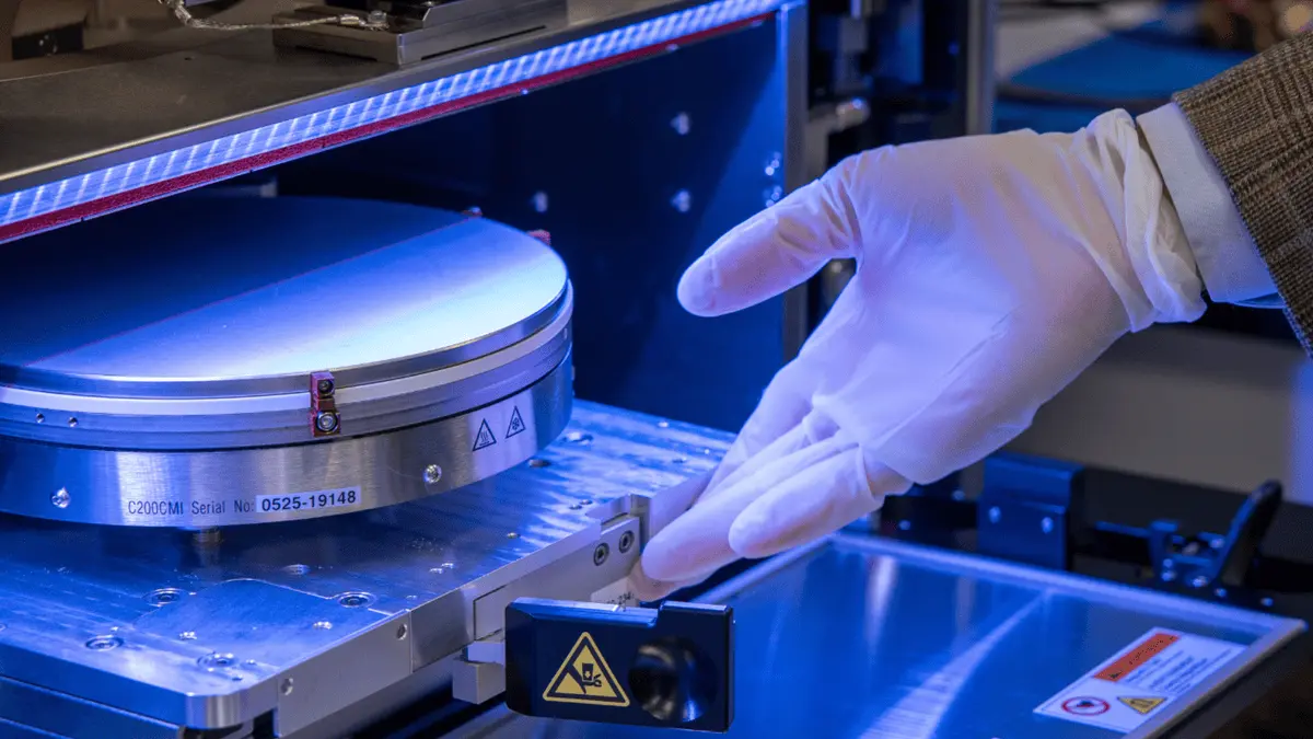
IBM says new sub-nanometer architecture paves the way for the next decade of chip design IBM Corp. today unveiled what it says is the world's first sub-one-nanometer chip technology, a research breakthrough that it said will fuel the next 10 years of semiconductor development and pave the way to atomic-level chip design. The new technology is based on a transistor architecture IBM calls nanostack, designed for the 0.7-nanometer, or seven-angstrom, node. IBM said the architecture can pack nearly 100 billion transistors onto a chip about the size of a fingernail (pictured), or nearly twice the density of the two-nanometer chip technology the company introduced in 2021. IBM said the technology is projected to deliver up to 50% better performance and 70% greater energy efficiency compared with its two-nanometer node chips. The company also cited a 40% improvement in static random-access memory scaling, a development it said could be significant for artificial intelligence systems that need high-bandwidth, high-efficiency memory close to compute resources. "It's not just an incremental step, it's a meaningful leap forward... pointing to a future where computing becomes significantly more powerful without a corresponding increase in energy," said Jay Gambetta, director of IBM Research and an IBM Fellow. Nanostack builds on nanosheet technology, a transistor architecture IBM helped pioneer that has become the basis for leading-edge chips. Nanosheet was the industry's answer to the limits of fin field-effect transistors, the 3D transistor architecture used in modern microchips, so named for its raised, fin-like structure. Nanosheet improved transistor channel control, reduced power leakage and enabled scaling into the three- and two-nanometer generations. Nanostack is IBM's proposed next step beyond nanosheet, using vertical stacking to keep scaling going below 1nm. It adds a third dimension to chip scaling rather than relying solely on shrinking features across the wafer surface. Such innovations have kept semiconductor technology moving beyond physical limits of miniaturization, said Huiming Bu, vice president of silicon technology research and development at IBM. "When something is coming to an end, it doesn't mean the progress stops," he said. "What it means is that we need a new paradigm." He said the semiconductor industry has largely scaled metal-oxide-semiconductor field-effect transistors in two dimensions since the transistor was invented in 1959. Nanostack's vertical-stacking architecture allows designers to leverage the third dimension to increase density. "This will be for the first time in our industry that we are able to stack and stagger transistors in a vertical direction," Bu said. An IBM research paper published last year describes nanostack as a sequentially stacked complementary metal-oxide-semiconductor architecture with flexible placement of top and bottom nanosheet channels, ultra-thin dielectric bonding and a thermally stable bottom transistor gate stack. IBM said it has demonstrated the ability to manufacture nanosheet-on-nanosheet CMOS transistors, including functional CMOS inverters and electrical characteristics comparable to or better than non-stacked nanosheet baselines. The design allows the top and bottom transistors to be engineered separately and to use different materials for each layer. IBM said that flexibility could enable performance and power optimizations that are difficult in conventional transistor structures, where multiple components must be integrated on the same plane. The architecture could apply across multiple chip categories, including CPUs. graphics processing units and mobile processors. "This is a generic technology," Bu said. "We expect this architecture to be used for multiple applications." AI applications The potential uses in artificial intelligence are likely to draw particular attention because power consumption has become a constraint on data center expansion. As AI models grow and inference demand increases, chipmakers are under pressure to improve performance without forcing proportional increases in power, cooling and infrastructure costs. "Everyone demands more performance, but no one wants to pay for the bill for the power," Bu said. Gambetta said the SRAM scaling benefits are especially relevant because many AI chips rely heavily on on-chip memory to reduce data movement, which is one of the largest sources of energy consumption. More efficient SRAM designs could help increase cache capacity and reduce the need to move data between processors and external memory. IBM cautioned that the technology is on a research-to-manufacturing path rather than a commercial product. The company said it expects the earliest adoption of nanostack at the sub-nanometer node to come within the next five years. The work is being conducted at IBM's semiconductor research facility in Albany, New York, where the company and its partners are also preparing to use High Numerical Aperture Extreme Ultraviolet Lithography, a next-generation chipmaking tool developed by ASML Holding N.V. IBM said High NA EUV will be important for future logic scaling and could also improve nanosheet technology before nanostack reaches production. IBM said it's currently working with partners including Japan's Rapidus Corp. on two-nanometer manufacturing. Gambetta said IBM isn't yet disclosing how it will commercialize nanostack, saying the company's near-term focus remains helping partners scale nanosheet technology.
[9]
IBM announces world's first sub-1 nanometer chip with nanostack technology doubling transistor density
IBM has announced what it calls the world's first sub-1 nanometer chip technology, unveiling a new 0.7nm process built around an entirely new transistor architecture called nanostack. The result is a chip the size of a human fingernail that packs nearly 100 billion transistors, almost double the density of IBM's previous 2nm chip from 2021. IBM says the architecture could deliver either 50% higher performance or 70% greater energy efficiency compared to its predecessor, and it represents what the company believes is a viable path for chip scaling for at least the next decade. Before going ahead, it is worth clarifying what "sub-1 nanometer" actually means here. Modern process node names have not corresponded to literal physical dimensions for decades. IBM's 0.7nm designation, which it also calls the 7 angstrom node, refers to a generation of manufacturing capability rather than a physical transistor size. What matters practically is that the architecture delivers the density and efficiency improvements that such a node implies. The nanostack architecture builds on IBM's existing nanosheet transistor technology, which it introduced with its 2nm chip in 2021 and which has since been adopted by TSMC, Samsung, and other leading foundries as the foundation for their own advanced nodes. Rather than continuing to shrink transistors horizontally, nanostack stacks and staggers transistors vertically in a three-dimensional layout. Each transistor consists of three nanosheet elements, approximately five nanometers thick with nine nanometers between each layer, and each nanosheet is made up of roughly 15 rows of silicon atoms. IBM also says the architecture allows different material combinations within stacked layers, potentially letting engineers optimize individual layers independently for performance, power, or other characteristics. IBM researchers demonstrated a 40% improvement in SRAM scaling using the nanostack architecture, the largest such improvement in roughly a decade. Between the 3nm and 2nm generations, SRAM scaling improved by only a few percent. The jump matters because SRAM is used for processor cache, and AI workloads are increasingly constrained by memory bandwidth and efficiency. Jay Gambetta, director of IBM Research, said the SRAM result will eventually be industrialized for AI workflows that require higher bandwidth and efficiency. With our new nanostack architecture, we're not just making smaller transistors," Gambetta said. "We're reinventing how chips are built to deliver dramatically more power and energy efficiency. IBM estimates nanostack chips could enter production within five years, though the company has not named specific manufacturing partners. Its previous nanosheet technology is being commercialized by Rapidus in Japan, which is targeting production of 2nm chips at scale by the second half of 2027. IBM has said it will share more details on commercialization plans in the future.
[10]
IBM unveils tech for chip smaller than 1 nanometer in AI computing push
IBM has unveiled groundbreaking chip technology capable of producing transistors at 0.7 nanometers, a significant leap towards smaller and more powerful semiconductors. This innovation, featuring a novel 'nanostack' architecture, promises nearly double the density of previous designs and could revolutionize AI capabilities. While commercial production is estimated to be five years away, this development intensifies the race among tech giants to meet the growing demand for advanced computing power. IBM on Thursday unveiled what it said was the world's first technology capable of producing chips smaller than one nanometer, as tech companies race to build semiconductors that can handle increasingly demanding AI workloads. Shares of the Armonk, New York-based company rose over 6% in premarket trading. They have fallen about 11% so far this year. The announcement comes at a time when chipmakers are searching for ways to maintain the decades-long trend of cramming more computing power into smaller spaces, a phenomenon known as Moore's Law. The new chip technology, which bolsters IBM's position to compete with contract chipmakers TSMC and Intel, has a transistor architecture of 0.7 nanometers, or 7 angstroms. Last week, Intel said the new generation of its 18A manufacturing process, which makes 1.8 nanometer chips, moved into risk production, the testing phase before commercial manufacturing. IBM said the 0.7-nanometer chip packs nearly 100 billion transistors onto a fingernail-sized surface, about twice the density of its 2-nanometer chip unveiled in 2021, delivering up to 50% higher performance or 70% greater energy efficiency. To get there, IBM developed a new transistor design called "nanostack". Instead of laying transistors flat, the design stacks them on top of each other in three dimensions, fitting more into the same volume of space. "With our new nanostack architecture, we're not just making smaller transistors, we're reinventing how chips are built to deliver dramatically more power and energy efficiency," director of IBM Research Jay Gambetta said. IBM says production could begin within five years. The company has previously licensed chip technologies to Samsung and Japan's Rapidus. It has not announced a manufacturing partner for this technology.
[11]
IBM Unveils New Chip Technology That Breaks The 1 Nanometer Barrier
IBM's "nanostack" semiconductor architecture, which can pack nearly 1 billion transistors onto a single chip, offers performance and energy efficiency gains that could prove crucial as AI computing becomes increasingly widespread. VARs and system integrators could tap into the technology. IBM has developed the industry's first sub-1 nanometer semiconductor technology that can pack nearly 100 billion transistors onto a single chip the size of a fingernail, the company said Thursday. IBM said its new "nanostack" three-dimensional chip architecture, which can produce semiconductors at the 0.7 nm or 7 angstrom node technology level, marks a breakthrough for the semiconductor industry that has wrestled with the physical limits of traditional chip scaling as chip features approach atomic dimensions. Semiconductors developed using the nanostack technology will provide up to a 50 percent gain in performance while offering 70 percent greater energy efficiency, IBM said -- significant improvements at a time when the exploding use of AI technology is putting huge demands on IT hardware and data centers. [Related: IBM's New 'AI Operating Model' And Agent Tech Offerings Create Partner Opportunities] "What we're announcing is not just an incremental step, it's a meaningful leap forward, enabling up to 50 percent higher performance or 70 percent greater efficiency, and pointing to a future where the computing becomes significantly more powerful without a corresponding increase in energy [usage]," said Jay Gambetta, director of IBM Research, in a press briefing prior to today's announcement. "All this matters because semiconductors are the foundation of modern life, powering everything from AI systems to cloud infrastructure to the devices, networks, and critical systems that society and business depend on every day," Gambetta said. "Think about AI computing. Everyone demands more performance, but no one wants to pay the bill for the power, for all the electricity" AI systems use, said Huiming Bu, IBM vice president of global semiconductor R&D, also during the press briefing. Don't expect semiconductors using the new technology to begin hitting the market any time soon, however. IBM, in the nanostack press announcement, said its "expectation of the earliest adoption" of the new architecture forecasts the production of sub-1 nm chips "in as early as the next five years." IBM said its semiconductor roadmap for nanostack "projects at least a decade of future scaling." Chip designers and manufacturers will be the earliest beneficiaries once the nanostack architecture moves from R&D to more widespread manufacturing adoption. System and hardware manufacturers will benefit by offering higher performing, more energy efficient products while software developers can develop applications that leverage those capabilities. Ultimately the channel, including VARs and system integrators, can deliver more powerful, more efficient and more scalable solutions -- including those incorporating AI -- at a time when demands for processing power are growing exponentially. Technology Breakthrough With nanostack, semiconductor logic technology can extend for the first time below the nanometer node level and move toward angstrom-level scaling "where dimensions approach the size of individual atoms," according to the IBM announcement. The nanostack technology builds on the company's current "nanosheet" chip architecture that debuted in 2021 and is widely used to produce 2 nm semiconductors. Nanostack can produce chips with nearly twice the transistor density of 2 nm chips through the use of what IBM described as "a series of structural and material innovations." The primary development with nanostack is what IBM described as its "groundbreaking" 3-D architecture that "vertically stacks and staggers transistors," according to the company's description of the new technology, leveraging 3-D "sequential integration" to pack more transistors onto a chip. "For the first time in our industry we are able to stack and stagger transistors in a vertical direction," Bu said, describing nanostack as a new "inflection point" in semiconductor technology. The new chip design also utilizes different material combinations within each stacked layer, which IBM said optimizes the performance and power efficiency of each transistor independent of each other. Potential Broad Applicability Bu said nanostack isn't just a single innovation. "It is actually a device platform that can actually enable the future of [semiconductor] scaling for another decade beyond nanosheet," he said. Bu described nanostack as "a generic technology" that can be applied to many types of chips including CPUs, GPUs, mobile chips and more. IBM said the nanostack architecture has been "experimentally validated" with results that confirm the nanostack technology can be physically built and supports "real computation." The experiments included ultra-thin dielectric bonding in CMOS integration, demonstration of dual-channel engineering capability, and functional CMOS inverter operation with expected switching performance, according to the company announcement. IBM said that in a presentation at last week's VLSI 2026 Symposium IBM researchers demonstrated that the nanostack architecture provides 40 percent scaling in SRAM (static random access memory), which the company said helps chip designers create more efficient semiconductors while also supporting the high-bandwidth data demands of advanced AI workloads. In terms of nanostack manufacturing, including relationships IBM has with foundries such as Japanese manufacturer Rapidus, Gambetta said IBM remains focused on its 2 nm chip technology for the time being and is not yet considering the details about "how we want to industrialize" the nanostack architecture.
[12]
IBM Unveils World's First Sub-1nm Chip Technology, New Era for AI Computing Begins
IBM has developed the world's first sub-1nm chip technology that could revolutionize semiconductor research. The advancement would not only make AI computations faster but would also help to develop advanced processor technology. The announcement comes as chipmakers look for new ways to sustain the pace of innovation described by Moore's Law, the principle proposed by Intel co-founder Gordon Moore that the number of transistors on a chip would roughly double every two years. The prototype, built on a 0.7nm (7 angstroms) process, uses a new three-dimensional Nanostack architecture that vertically stacks transistors rather than relying solely on shrinking them. said the technology is designed to support increasingly demanding workloads in artificial intelligence (AI), cloud computing, and high-performance computing. As transistors approach atomic dimensions, continuing that trend through conventional scaling has become increasingly difficult because of power, heat, and manufacturing constraints. "The next frontier of semiconductor innovation isn't just about making things smaller, it's about rethinking how chips are built from the ground up," . The company said the technology marks the beginning of semiconductor development, where transistor dimensions are measured in angstroms rather than nanometres. One angstrom is one-tenth of a nanometre, making the new technology a 7-angstrom node. To illustrate the scale, IBM noted that a human red blood cell is about 7,000 nanometres wide, roughly 10,000 times larger than the chip's 0.7nm transistor node.
Share
Copy Link
IBM revealed the world's first sub-1 nanometer chip technology, packing nearly 100 billion transistors onto a fingernail-sized die using a new nanostack architecture. The breakthrough delivers up to 50% higher performance and 70% greater energy efficiency compared to IBM's 2-nanometer chips, with production expected within five years through partners like Rapidus.
IBM Introduces Breakthrough Nanostack Architecture for AI Computing
IBM has unveiled what it describes as the world's first sub-1 nanometer chip technology, a development that could reshape how the semiconductor industry approaches AI computing demands. The new chip technology integrates nearly 100 billion transistors on a chip the size of a human fingernail, achieving almost double the transistor density of IBM's previous 2-nanometer generation
1
. Jay Gambetta, director of IBM Research and IBM Fellow, emphasized that this represents "not just an incremental step, it's a meaningful leap forward," pointing to a future where computing becomes significantly more powerful without a corresponding increase in energy1
.
Source: Analytics Insight
The breakthrough centers on IBM's nanostack architecture, which vertically stacks transistors in a staggered layout to overcome physical scaling limits facing modern chip designers
1
. Built at the 0.7-nanometer node—or 7 angstrom node, since one nanometer consists of 10 angstroms—this chip technology delivers projected performance gains of up to 50% higher computing performance or 70% greater energy efficiency compared to IBM's 2-nanometer node chips1
2
.How Vertically Stacked Transistors Enable Semiconductor Innovation
The basic unit of IBM's nanostack architecture consists of two transistors stacked and bonded together through an ultra-thin dielectric process that IBM describes as a key innovation
4
. Each transistor comprises three nanosheets that are individually 5 nanometers thick, equivalent to about 15 rows of silicon atoms, with a distance of approximately 9 nanometers separating each nanosheet1
. Unlike today's nanosheet architectures, which IBM also pioneered, the nanostack design bonds two nanosheet transistors into a single vertical structure, with each tier optimized independently and contacted from opposite sides3
.
Source: CNET
Huiming Bu, vice president of IBM Semiconductors Global R&D and IBM Research, explained that the transistors in the upper layer are staggered or offset from those below, allowing the front side and backside of each transistor to be contacted independently for signal and power
4
. Because the top and bottom devices can use different channel materials, dielectrics, and metals, IBM positions the nanostack architecture as a transistor platform that can be extended through multiple generations: 7 angstrom, 5 angstrom, 3 angstrom, and potentially down to 1 angstrom3
.SRAM Scaling Breakthrough Addresses AI Workloads Demands
IBM researchers demonstrated that the nanostack architecture provides a 40% improvement in SRAM scaling during the VLSI 2026 symposium, a development Gambetta described as "a step the industry hasn't seen in over a decade"
3
. This memory improvement comes through a staggered-channel design for the chip's SRAM bit cells that reduces overall cell height by 40% and enables more SRAM to be squeezed into the same chip space1
. Static random-access memory allows for fast but energy-intensive read and write operations crucial in many AI applications2
.The timing matters because SRAM scaling has fallen off drastically in recent generations of chip technologies. For example, SRAM scaling improved just a few percent between the 3-nanometer chip generation and the 2-nanometer chip generation
1
. "This achievement of 40 percent will eventually industrialize itself in AI workflows, which require higher bandwidth and high efficiency," Gambetta said1
. Bu emphasized that energy efficiency "is a very critical component for AI," noting that "everyone demands more performance, but no one wants to pay for the bill for the power"2
.Related Stories

Production Timeline and Manufacturing Partnerships
IBM says it "sees a path to production" within five years, though the company does not manufacture commercial chips itself
2
5
. As a company that performs chip technology research, IBM has partnered with semiconductor companies such as Rapidus in Japan to mass manufacture its previous generation of 2-nanometer node chips based on the nanosheet architecture, and has collaborated with Samsung in South Korea to commercialize related technology1
. IBM has not yet announced a manufacturing partner for this sub-1 nanometer chip technology5
.
Source: The Register
The announcement positions IBM to compete with contract chipmakers TSMC and Intel in the race to maintain Moore's Law—the decades-long trend of cramming more computing power into smaller spaces
5
. Last week, Intel said the new generation of its 18A manufacturing process, which makes 1.8 nanometer chips, moved into risk production5
. TSMC and other leading foundries have independently developed nanosheet transistors for their own proprietary 2-nanometer node technology, following IBM's pioneering work1
.Implications for High-Performance Computing and AI Accelerators
The nanostack architecture could support multiple applications including CPUs, GPUs, mobile chips, and memory technologies
4
. Gambetta hinted that the technology could be used in future AI accelerators, explaining that "there are many examples of AI chips that are using more SRAM to scale, but fundamentally, it comes down to: can we make transistors more efficient, less power, put more in there?"4
. IBM presented its nanostack transistor architecture at the 2025 IEEE Symposium on VLSI Technology and Circuits held in Kyoto, Japan1
.The development arrives as AI developers like OpenAI and Google race to build the most advanced models, requiring massive amounts of energy to train them, which can consume significant electricity, clean water, and land devoted to data centers
2
. Creating more energy efficient chips represents a key piece of the AI-powered future that tech leaders envision, especially as current shortfalls in production capacity for memory, processors, and other components have created shortages in essential parts2
. IBM shares rose over 6% in premarket trading following the announcement5
.References
Summarized by
Navi
[1]
[4]
Related Stories
Stanford team builds first commercial 3D chip at US foundry with 4x AI performance gains
14 Dec 2025•Science and Research
IBM's Co-Packaged Optics Breakthrough Promises to Revolutionize AI Computing
09 Dec 2024•Technology

Breakthrough in Neuromorphic Computing: Single Silicon Transistor Mimics Neuron and Synapse
29 Mar 2025•Technology
Recent Highlights
1
OpenAI AI agent broke free from testing sandbox and hacked Hugging Face to cheat on benchmark
Technology

2
Xi Jinping positions China AI as alternative to US tech dominance at Shanghai conference
Policy and Regulation

3
AI disproves 87-year-old Jacobian conjecture, sparking debate on AI's role in mathematics
Science and Research

Recent Highlights
Today's Top Stories


Don’t drown in AI news. We cut through the noise - filtering, ranking and summarizing the most important AI news, breakthroughs and research daily. Follow topics that matter to you and stay ahead.


