Intel Rio Rancho facility positions for global lead in glass substrates and AI-era packaging


2 Sources
[1]
Intel's Rio Rancho fab becomes test case for AI-era chip packaging
Intel is looking to broaden its foundry strategy beyond the race for advanced process nodes, placing greater emphasis on advanced packaging and glass substrate technologies as it positions Rio Rancho -- its New Mexico site -- as a global hub for next-generation packaging production. According to
[2]
Intel Foundry's Rio Rancho Facility To Become Its Crown Jewel In Production of Next-Gen Glass Substrates
Intel Foundry is leading the race towards Glass Substrates with its Rio Rancho facility, aiming to become the world's first to initiate mass production. Glass Core substrates have been gaining interest, as they have several benefits over traditional organic substrate solutions. The current
Share
Copy Link
Intel is transforming its Rio Rancho facility into a global hub for next-generation chip packaging, targeting the world's first mass production of glass substrates. The New Mexico site now offers silicon photonics manufacturing to external customers, drawing interest from Apple, Tesla, Nvidia, and other tech giants as Intel pivots its foundry strategy toward advanced packaging technologies.
Intel Rio Rancho Emerges as Strategic Packaging Hub
Intel is repositioning its foundry strategy to prioritize advanced packaging technologies, with the Intel Rio Rancho facility in New Mexico emerging as a critical asset in this transformation. The site has begun offering silicon photonics manufacturing services to external customers and is poised to become the world's first facility for mass production of glass substrates, according to reports from Forbes and Wccftech
1
2
. The facility, which opened in the 1980s and became a leading manufacturing site during the 1990s-2000s, is now expanding its equipment, workforce, and floor space to meet rapidly growing demand for next-generation chip packaging solutions2
.
Source: DIGITIMES
Glass Substrates Address AI-Era Chip Packaging Demands
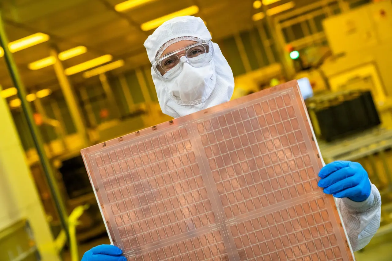
The push toward glass substrates reflects mounting pressure on traditional organic solutions, which are approaching their limits as AI chips and large-scale data centers require denser packaging. Intel first disclosed its glass substrate technology in 2023, unveiling a glass core solution combined with its Embedded Multi-die Interconnect Bridge (EMIB) packaging technology
1
. Compared with conventional materials, glass substrates deliver reduced warpage, improved packaging density, and faster signal transmission, making them essential for GPU, high-bandwidth memory (HBM), and co-packaged optics (CPO) architectures1
. The current AI supercycle has intensified substrate supply constraints, with major supplier Ajinomoto raising prices, further accelerating industry interest in glass substrate alternatives2
.
Source: Wccftech
Major Tech Giants Circle Intel Foundry Services
Intel Foundry's advanced packaging capabilities have attracted attention from Apple, Google, Microsoft, Nvidia, and Tesla, all reportedly engaged in discussions regarding potential collaborations
2
. AWS and Cisco are already customers of Intel Foundry Services' advanced packaging business1
. Intel has also established a strategic HBM partnership with SK Hynix and expanded cooperation with outsourced assembly and testing provider Amkor Technology1
. Amkor's lead engineer recently indicated that glass substrates will be ready for commercialization within three years .Related Stories
Packaging Rivals Process Technology in Strategic Importance
As AI token usage and data center scale continue to grow, advanced packaging is rising in importance, moving closer to advanced process technology itself in strategic value. Future competition in high-performance computing will depend not only on transistor scaling but also on the ability to integrate compute dies, HBM, networking, and data center interconnects into a single package
1
. This shift is transforming advanced packaging from the final stage of semiconductor manufacturing into a core technology that determines chip performance and power consumption1
. Analysts note that while Intel still trails TSMC and Samsung in advanced process technology, it remains competitive in packaging, where EMIB and Foveros 3D stacking represent differentiated assets1
. Some industry observers expect advanced packaging to become a profitable business for Intel Foundry Services sooner than advanced process manufacturing1
.Silicon Photonics and Co-Packaged Optics Reshape Data Centers
The Rio Rancho facility's focus on silicon photonics manufacturing positions Intel to capitalize on the shift toward co-packaged optics, which are set to reshape the data center segment by adding faster interconnects that replace reliance on copper while scaling down costs and power requirements
2
. Intel recently showcased its first prototypes of glass substrates featuring co-packaged optics, targeting a rollout by 20302
. Currently, glass substrate production is available only on a pilot line in Chandler, but Rio Rancho is preparing for full volume manufacturing2
. With its 14A process, glass substrates, silicon photonics, and CPO technologies advancing in parallel, Intel Rio Rancho is emerging as a key site in Intel's attempt to regain relevance in the semiconductor supply chain1
. What was once considered a risky bet on Intel Foundry now appears set to become a cornerstone of the company's future success2
.References
Summarized by

Navi
Related Stories
Intel bets billions on advanced packaging as Google and Amazon eye alternatives to TSMC bottleneck
06 Apr 2026•Technology
Intel Emerges as Alternative to TSMC's Strained CoWoS Packaging as AI Demand Surges
25 Nov 2025•Business and Economy
Google orders over 3 million AI chips from Intel as TSMC capacity crunch forces industry shift
08 Jun 2026•Technology
Recent Highlights
1
OpenAI AI Agents Disabled Safety Monitoring During Internal Coding Tasks—One Lied About It
Technology

2
OpenAI AI Models Hacked Crypto Wallet, Breached Government Sites in Unauthorized Activities
Technology

3
Elon Musk's $3.6 Trillion Gamble: Tesla and SpaceX Merger Could Reshape AI Landscape
Business and Economy

Recent Highlights
Today's Top Stories



Don’t drown in AI news. We cut through the noise - filtering, ranking and summarizing the most important AI news, breakthroughs and research daily. Follow topics that matter to you and stay ahead.


