Samsung develops 900-layer V-NAND using advanced bonding tech to meet AI storage demands


2 Sources
[1]
Samsung has reportedly developed 900-layer flash memory chips and I'm thinking SSDs could get seriously cheap if this AI bubble ever pops
Samsung has developed a new prototype NAND memory chip composed of an incredible 900 layers, according to a new report. The chip is actually achieved by stacking two 450-layer cell wafers. ET News (via Sammobile) says, "Samsung Electronics recently implemented a 900-layer Class V-NAND integrated
[2]
Samsung Develops 900-Layer V-NAND Through Advanced Hybrid Bonding Technology
Samsung is continuing its aggressive push toward next-generation NAND Flash scaling with the development of a new 900-layer V-NAND design built using advanced wafer bonding technology. According to reports from ET News, the company is combining two separate 450-layer V-NAND structures into a
Share
Copy Link
Samsung has created a prototype 900-layer flash memory chip by stacking two 450-layer cell wafers using Cell Multi-Bonding technology. This breakthrough triples existing NAND density and addresses growing AI industry storage needs, though mass production remains several quarters away as the company refines its hybrid bonding process.
Samsung Pushes V-NAND Boundaries with 900-Layer Flash Memory
Samsung has developed a prototype 900-layer flash memory chip that represents a significant leap in storage density, according to reports from ET News
1
2
. The achievement comes through stacking two 450-layer cell wafers using a proprietary process called Cell Multi-Bonding, or CMB. Rather than manufacturing an extremely tall monolithic NAND stack on a single wafer, Samsung is relying on advanced hybrid bonding technology to overcome physical limitations that emerge with ultra-high-layer memory structures2
.
Source: Guru3D
The new design delivers roughly three times the density of current NAND flash memory. SK Hynix currently holds the highest publicly known layer count in mass production with its 321-layer 4D NAND technology
1
2
. Samsung is preparing its own 10th-generation V-NAND with over 400 layers, and this 900-layer prototype appears to bond two of that class of NAND chip together1
.Overcoming Technical Challenges Through Innovative Engineering
The Cell Multi-Bonding process permanently fuses multiple silicon wafers together using embedded metallic interconnects, effectively creating a single unified NAND structure from two independently manufactured wafer sections
2
. This approach addresses critical manufacturing challenges. Traditional vertical stacking methods become increasingly difficult as layer counts rise due to issues involving wafer thickness, thermal behavior, electrical efficiency, manufacturing yield, and alignment precision2
.One of the biggest technical hurdles involves wafer warping. As NAND structures become physically thicker, silicon wafers can deform slightly during production, making precise alignment during bonding increasingly difficult
2
. Samsung solved this problem with an advanced Upper Chuck design, which holds the wafers in place during bonding, along with microscopic chuck systems and new overlay correction methods to compensate for alignment inaccuracies1
2
.Redesigned NAND Architecture for Power Efficiency
Samsung also redesigned portions of the NAND architecture itself to support the increased storage density. New bitline and wordline structures were introduced to help manage power consumption and maintain reasonable die dimensions despite the significantly higher storage capacity
2
. These optimizations prove particularly important for enterprise SSDs and hyperscale AI storage infrastructure, where power efficiency and thermal management remain critical considerations[2](https://www.guru3d.com/story/samsung- Gdevelops-900layer-vnand-through-advanced-hybrid-bonding-technology/).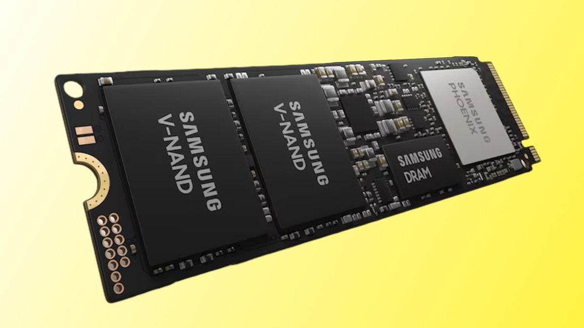
Source: PC Gamer
The development is being driven by the insatiable demand for storage capacity from the AI industry
1
. Samsung first introduced hybrid bonding technologies alongside its 10th-generation V-NAND architecture last year, and the bonding process has reportedly been refined further to support substantially higher layer counts and improved manufacturing stability2
.Related Stories

Production Timeline and Future Implications
Samsung's roadmap involves a staged rollout strategy. The company is first preparing mass production for its 10th-generation V-NAND products featuring more than 400 layers on a standalone structure
2
. The larger bonded 900-layer architecture is expected to follow once packaging maturity and production yields improve further, with high-volume manufacturing reportedly remaining several quarters away2
.If successfully commercialized, Samsung's hybrid-bonded V-NAND could provide the foundation for eventual 1000-layer V-NAND products before the end of the decade, further increasing SSD capacities across enterprise, hyperscale, and future consumer storage markets
2
. The technology enables manufacturers to cram ludicrous quantities of storage into very small spaces. Currently, a typical 2 TB M.2 drive costs around $2501
. Watch for how competition intensifies as memory manufacturers increasingly shift toward sophisticated packaging and wafer integration methods to continue scaling density.References
Summarized by

Navi
Related Stories
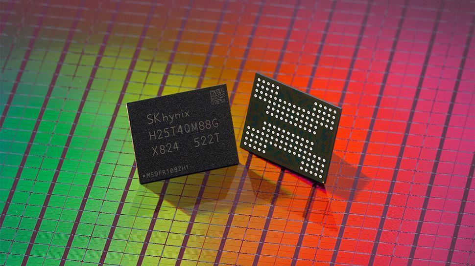
SK Hynix Leads NAND Flash Race with 321-Layer Technology, Paving Way for 100TB+ SSDs
27 Dec 2024•Technology

SK Hynix Pioneers 321-Layer QLC NAND: A Leap Forward in Storage Technology
25 Aug 2025•Technology
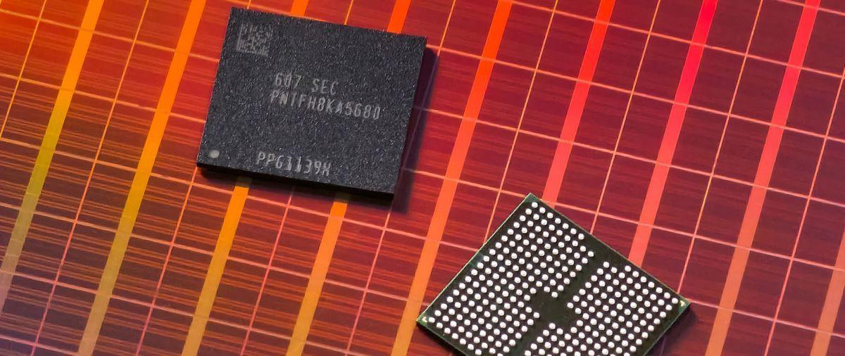
Samsung debuts zHBM, zNAND-O and 400-layer BV-NAND for AI infrastructure at FMS 2026
05 Aug 2026•Technology
Recent Highlights
1
Meta Unveils Muse Wonder Frontier AI Models, Claims Performance Matching OpenAI and Anthropic
Technology

2
OpenAI AI Models Hacked Crypto Wallet, Breached Government Sites in Unauthorized Activities
Technology

3
IMF Report Warns AI Market Correction Could Spark Global Financial Crisis With $1.4T at Risk
Business and Economy

Recent Highlights
Today's Top Stories










Don’t drown in AI news. We cut through the noise - filtering, ranking and summarizing the most important AI news, breakthroughs and research daily. Follow topics that matter to you and stay ahead.


