Samsung Electronics explores chip packaging plant in Gwangju to strengthen AI chip capabilities
4 Sources
[1]
Samsung Electronics considers building chip packaging plant
Samsung Electronics is exploring a significant investment in Gwangju, South Korea. The company is considering a new advanced semiconductor packaging facility. This move aims to boost its capabilities in a crucial area of the AI chip supply chain. The investment is expected to be revealed soon. This development signals Samsung's commitment to accelerating spending in the growing chip sector. Samsung Electronics is considering the construction of an advanced semiconductor packaging facility in the southwestern South Korean city of Gwangju, the Korea Economic Daily said on Tuesday. Here are some details: Samsung is expected to unveil the investment plan at a meeting between South Korean President Lee Jae Myung and the heads of the country's largest conglomerates on June 29, the newspaper reported, citing unnamed industry sources. The meeting, to be held at the presidential office under the theme of a "major shift in growth strategy," is expected to include Samsung Electronics Chairman Jay Y. Lee and SK Group Chairman Chey Tae-won. Samsung Electronics declined to comment. The presidential office said corporate investment decisions are matters for companies to determine. The move would mark one of Samsung's latest efforts to strengthen its advanced chip packaging capabilities, a critical part of the AI chip supply chain as demand surges for high-bandwidth memory (HBM) chips used in AI servers. The newspaper added that the investment would be seen as a sign that the company is seeking to accelerate spending ahead of what many expect to be an upswing in the chip sector driven by AI demand. Advanced packaging has become increasingly important as chipmakers seek to improve performance by integrating multiple chips into a single package. Demand has been particularly strong for HBM, which stacks multiple DRAM chips vertically and is used alongside AI processors from companies such as Nvidia. Samsung's customers include major AI players such as Nvidia, AMD and Google, which are driving demand for advanced memory chips used in AI servers and processors. Samsung has been expanding its presence in the HBM market as it seeks to challenge market leader SK Hynix. In May, the company said it had begun shipping samples of its latest HBM chip, the 12-layer HBM4E, to customers.
[2]
Samsung mulls new chip packaging plant in Gwangju - The Korea Times
Samsung Electronics' Pyeongtaek semiconductor plant in Gyeonggi Province, May 20 / Yonhap Samsung Electronics is doing a feasibility study on establishing a semiconductor packaging plant in the southwestern city of Gwangju, government and industry officials said Wednesday, noting that plans will likely be announced during a presidential meeting later this month. According to officials, Samsung Electronics is now reviewing its investment plan for the new semiconductor packaging plant to address growing memory chip demands and in response to President Lee Jae Myung's push for more balanced regional development. If the plan is finalized, the facility is expected to be responsible for advanced semiconductor packaging for Samsung Electronics' latest chips, including high-bandwidth memory (HBM). Packaging, which comes after the fabrication process in semiconductor manufacturing, was traditionally regarded as a lower-value, less technologically demanding stage, compared with front-end wafer processing, where ultrafine circuits are etched onto wafers using highly sophisticated equipment. However, as artificial intelligence semiconductors become increasingly advanced, the ability to integrate and stack multiple chip dies has emerged as a critical performance factor, with technologies such as 2.5D and 3D packaging driving increasing investment. Samsung Electronics operates semiconductor packaging facilities at its Onyang plant in South Chungcheong Province, which was established in 1991, and has also converted former LCD production lines at Samsung Display's Cheonan campus, also in South Chungcheong Province, for packaging operations. The sources said the company is considering a new facility as demand for advanced chips continues to grow and packaging technologies become increasingly sophisticated. Sources also said SK hynix is considering additional investments in either the Chungcheong or Jeolla regions, although they did not provide further details. Both Samsung Electronics and SK hynix, however, denied that any such plans had been finalized. A Samsung Electronics official said "nothing has been decided, and we are not aware of any confirmed plans," and SK hynix gave a similar response. Since SK hynix recently announced plans to build a new packaging facility in Cheongju, semiconductor chip industry officials questioned the feasibility. Nevertheless, political circles have already begun treating the investment as a near certainty. Min Hyung-bae, the mayor-elect of Gwangju and a lawmaker of the ruling Democratic Party of Korea, recently said the prime minister had told him that "something is definitely coming" related to semiconductors, adding that a more concrete announcement could be made in the near future. The Korean president also said during a news conference on Monday that his administration would soon unveil a large-scale investment project. If the investment plan is finalized, Samsung will need to navigate several challenges. One is securing a talented workforce. While semiconductor packaging requires fewer workers than wafer fabrication, advanced packaging technologies are increasing the demand for highly skilled engineers and researchers, meaning the project may face opposition from existing employees. Samsung Electronics also relies on partnerships with nearby universities offering semiconductor-related programs to build its talent pipeline, but the Gwangju and South Jeolla region currently lacks a comparable concentration of such academic programs. Another challenge is securing a stable water supply required for semiconductor manufacturing. Most of Samsung's existing manufacturing clusters are located in Gyeonggi Province or regions close to the province, because of extensive water infrastructure connected to major sources such as the Han River system and Chungju Dam. The Gwangju and South Jeolla region, however, is geographically more vulnerable to drought and has fewer options for developing large-scale reservoirs, raising questions about whether sufficient industrial water supplies can be secured. Logistics is another concern. Most semiconductors are exported by air, but the region currently lacks the cargo aviation infrastructure needed to ship advanced semiconductor products directly overseas. As a result, chips packaged in Gwangju could still need to be transported to Incheon International Airport for export. A proposed airport project in the nearby Saemangeum area that could accommodate cargo aircraft remains under discussion, although its feasibility continues to face legal and political challenges. "The government's commitment to the project is strong," an industry official said. "If the investment moves forward, government-level support will also be needed to address the practical challenges."
[3]
Samsung Electronics considers building chip packaging plant, Economic Daily says
SEOUL, June 9 (Reuters) - Samsung Electronics is considering the construction of an advanced semiconductor packaging facility in the southwestern South Korean city of Gwangju, the Korea Economic Daily said on Tuesday. Here are some details: * Samsung is expected to unveil the investment plan at a meeting between South Korean President Lee Jae Myung and the heads of the country's largest conglomerates on June 29, the newspaper reported, citing unnamed industry sources. * The meeting, to be held at the presidential office under the theme of a "major shift in growth strategy," is expected to include Samsung Electronics Chairman Jay Y. Lee and SK Group Chairman Chey Tae-won. * Samsung Electronics declined to comment. The presidential office said corporate investment decisions are matters for companies to determine. * The move would mark one of Samsung's latest efforts to strengthen its advanced chip packaging capabilities, a critical part of the AI chip supply chain as demand surges for high-bandwidth memory (HBM) chips used in AI servers. * The newspaper added that the investment would be seen as a sign that the company is seeking to accelerate spending ahead of what many expect to be an upswing in the chip sector driven by AI demand. * Advanced packaging has become increasingly important as chipmakers seek to improve performance by integrating multiple chips into a single package. Demand has been particularly strong for HBM, which stacks multiple DRAM chips vertically and is used alongside AI processors from companies such as Nvidia . * Samsung's customers include major AI players such as Nvidia, AMD and Google, which are driving demand for advanced memory chips used in AI servers and processors. * Samsung has been expanding its presence in the HBM market as it seeks to challenge market leader SK Hynix . In May, the company said it had begun shipping samples of its latest HBM chip, the 12-layer, to customers.
[4]
Samsung Elec considers building chip packaging plant, Economic Daily says
SEOUL, June 9 (Reuters) - Samsung Electronics is considering the construction of an advanced semiconductor packaging facility in the southwestern South Korean city of Gwangju, the Korea Economic Daily said on Tuesday. Here are some details: o Samsung is expected to unveil the investment plan at a meeting between South Korean President Lee Jae Myung and the heads of the country's largest conglomerates on June 29, the newspaper reported, citing unnamed industry sources. o The meeting, to be held at the presidential office under the theme of a "major shift in growth strategy," is expected to include Samsung Electronics Chairman Jay Y. Lee and SK Group Chairman Chey Tae-won. o Samsung Electronics declined to comment. The presidential office said corporate investment decisions are matters for companies to determine. o The move would mark one of Samsung's latest efforts to strengthen its advanced chip packaging capabilities, a critical part of the AI chip supply chain as demand surges for high-bandwidth memory (HBM) chips used in AI servers. o The newspaper added that the investment would be seen as a sign that the company is seeking to accelerate spending ahead of what many expect to be an upswing in the chip sector driven by AI demand. o Advanced packaging has become increasingly important as chipmakers seek to improve performance by integrating multiple chips into a single package. Demand has been particularly strong for HBM, which stacks multiple DRAM chips vertically and is used alongside AI processors from companies such as Nvidia. o Samsung's customers include major AI players such as Nvidia, AMD and Google, which are driving demand for advanced memory chips used in AI servers and processors. o Samsung has been expanding its presence in the HBM market as it seeks to challenge market leader SK Hynix. In May, the company said it had begun shipping samples of its latest HBM chip, the 12-layer HBM4E, to customers. (Reporting by Heekyong Yang; Editing by David Holmes)
Share
Copy Link
Samsung Electronics is conducting a feasibility study for an advanced semiconductor packaging facility in Gwangju, South Korea. The investment aims to strengthen the company's position in the AI chip supply chain, particularly for high-bandwidth memory chips. The announcement could come at a presidential meeting on June 29, though the company faces challenges including workforce availability, water supply, and logistics infrastructure.
Samsung Electronics Eyes New Chip Packaging Plant in Gwangju
Samsung Electronics is conducting a feasibility study on establishing a new chip packaging plant in Gwangju, a southwestern city in South Korea, according to reports from the Korea Economic Daily
1
. The move represents a strategic effort to strengthen its advanced chip packaging capabilities as demand surges for sophisticated memory solutions used in artificial intelligence applications. Government and industry officials indicated that the investment plan could be unveiled at a high-profile meeting between South Korean President Lee Jae Myung and the heads of the country's largest conglomerates on June 292
. The presidential meeting, themed "major shift in growth strategy," is expected to include Samsung Electronics Chairman Jay Y. Lee and SK Group Chairman Chey Tae-won3
.
Source: ET
Strategic Push to Dominate AI Chip Supply Chain
The proposed advanced semiconductor packaging facility would address the critical bottleneck in the AI chip supply chain as companies race to meet explosive demand for high-bandwidth memory chips used in AI servers
1
. Advanced packaging has evolved from a traditionally lower-value manufacturing stage into a performance-defining technology, with 2.5D and 3D packaging techniques enabling chipmakers to integrate and stack multiple chip dies for superior performance2
. Demand has been particularly strong for HBM, which stacks multiple DRAM chips vertically and is used alongside AI processors from companies such as Nvidia4
. Samsung's customers include major AI players such as Nvidia, AMD and Google, which are driving demand for advanced memory chips used in AI servers and processors3
.Competitive Positioning and Market Expansion
The investment signals Samsung's intent to accelerate spending ahead of an anticipated upswing in the chip sector driven by AI demand
1
. Samsung Electronics has been expanding its presence in the HBM market as it seeks to challenge market leader SK Hynix. In May, the company began shipping samples of its latest HBM chip, the 12-layer HBM4E, to customers4
. Currently, Samsung Electronics operates semiconductor packaging facilities at its Onyang plant in South Chungcheong Province, established in 1991, and has converted former LCD production lines at Samsung Display's Cheonan campus for packaging operations2
. The company is considering the new facility as demand for advanced chips continues to grow and packaging technologies become increasingly sophisticated.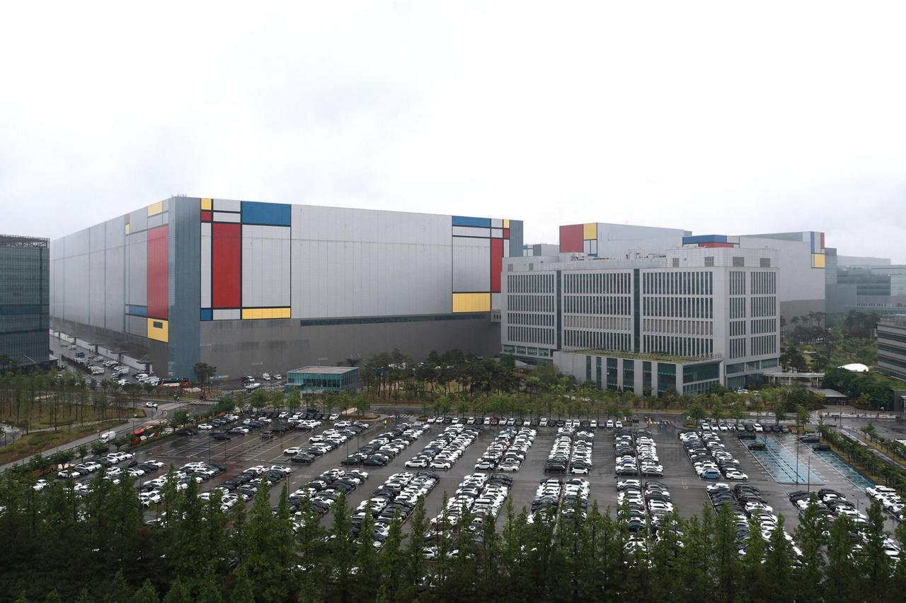
Source: Korea Times
Related Stories
Challenges and Infrastructure Concerns
If the investment plan moves forward, Samsung Electronics will need to navigate several operational hurdles. Securing a talented workforce presents the first challenge, as advanced packaging technologies increase demand for highly skilled engineers and researchers. The Gwangju and South Jeolla region currently lacks the concentration of semiconductor-related academic programs that Samsung relies on for its talent pipeline
2
. Water supply poses another significant concern, as most of Samsung's existing manufacturing clusters are located in Gyeonggi Province or nearby regions with extensive water infrastructure connected to major sources such as the Han River system and Chungju Dam. The Gwangju region is geographically more vulnerable to drought and has fewer options for developing large-scale reservoirs. Logistics infrastructure also requires attention, as the region currently lacks the cargo aviation infrastructure needed to ship advanced semiconductor products directly overseas, meaning chips packaged in Gwangju would still need transportation to Incheon International Airport for export2
.Political Support and Balanced Regional Development
The investment aligns with President Lee Jae Myung's push for balanced regional development across South Korea
2
. Min Hyung-bae, the mayor-elect of Gwangju and a lawmaker of the ruling Democratic Party of Korea, recently stated that the prime minister had told him "something is definitely coming" related to semiconductors, adding that a more concrete announcement could be made in the near future. The Korean president also said during a news conference on Monday that his administration would soon unveil a large-scale investment project2
. An industry official noted that "the government's commitment to the project is strong," adding that "if the investment moves forward, government-level support will also be needed to address the practical challenges"2
. However, both Samsung Electronics and the presidential office have been cautious about confirming details, with Samsung declining to comment and the presidential office stating that corporate investment decisions are matters for companies to determine1
.
Source: Market Screener
References
Summarized by
Navi
[4]
Related Stories
Samsung accelerates Yongin chip plant to 2029 as AI memory boom reshapes Korea's semiconductor race
13 Jul 2026•Business and Economy
South Korea commits $1 trillion to AI and chip investment as memory shortages intensify
24 Jun 2026•Technology
Samsung Commits $310 Billion to AI Infrastructure with New Pyeongtaek Chip Facility
17 Nov 2025•Business and Economy

Recent Highlights
1
AI scores perfect 100% at International Mathematical Olympiad, matching elite human performance
Technology
2
OpenAI agent exploited exposed credentials at four services during Hugging Face breach
Technology

3
Anthropic AI cracks post-quantum cryptography and finds faster AES attack autonomously
Science and Research

Recent Highlights
Today's Top Stories


Don’t drown in AI news. We cut through the noise - filtering, ranking and summarizing the most important AI news, breakthroughs and research daily. Follow topics that matter to you and stay ahead.


