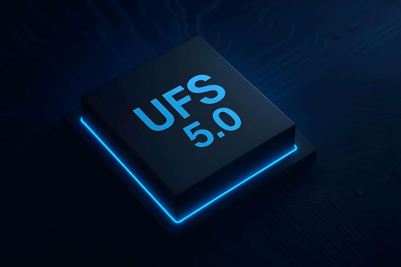
Samsung unveils UFS 5.0 storage with 10.8GB/s speeds to accelerate on-device AI workloads
10 Sources
[1]
Samsung shows off ultra-fast UFS 5.0 storage for flagship phones and on-device AI
Serving tech enthusiasts for over 25 years. TechSpot means tech analysis and advice you can trust. In context: Universal Flash Storage is a solid-state storage standard developed by JEDEC in collaboration with major memory industry players. Designed as a successor to eMMC storage and external SD cards, UFS has evolved to deliver performance levels that rival those of some PC storage solutions. Samsung is now looking to leverage that performance to accelerate AI workloads on next-generation smartphones. Samsung has announced its Universal Flash Storage 5.0 chips, a flash-based storage solution designed primarily for smartphones, tablets, and other mobile devices. The UFS 5.0 standard delivers a maximum bandwidth of 10.8 GB/s and is positioned as a way to accelerate on-device AI workloads. Based on the JEDEC-developed UFS interface standard, the technology uses two data lanes to achieve sequential read speeds of up to 10.8 GB/s, while sequential write speeds can reach up to 9.5 GB/s. Samsung claims these chips deliver the highest performance in the mobile storage segment, more than doubling sequential speeds compared to UFS 4.1. The UFS 5.0 packages measure 7.5 mm × 13 mm × 0.9 mm, making them about 16.7% smaller than UFS 4.1 solutions. The reduced footprint could enable more flexible device designs by improving internal space efficiency for storage components. Additional improvements in UFS 5.0 include a reported 40% increase in power efficiency, achieved through techniques such as clock gating and multi-voltage operation. As a result, devices can transfer the same amount of data while consuming significantly less energy, which could translate into improved battery life in next-generation mobile products. Samsung also emphasizes UFS 5.0's role in supporting on-device AI workloads, including offline chatbots and large language models. According to Jangseok Choi, head of memory product planning at Samsung Electronics, storage has become a critical component of emerging AI-driven computing systems. The company points to examples such as repurposed older Pixel devices used in low-cost data center setups as evidence of growing demand for efficient local storage performance. Samsung is expected to begin mass production of UFS 5.0 chips in the fourth quarter. Capacities will scale up to 1TB per chip, and the company aims to maintain a competitive edge in the flash storage market. Devices such as smartphones, XR headsets, and AI-enabled wearables featuring UFS 5.0 are expected to arrive later, although they are unlikely to come at lower price points.
[2]
Samsung Unveils Industry's Fastest UFS 5.0 Solution for Next-Gen On-Device AI Applications
Samsung's UFS 5.0 solution achieves the industry's highest data transfer speed of 10.8GB/s, enabling faster storage and processing in mobile memory Enhanced power efficiency and smaller package to provide optimal mobile AI experiences Samsung Electronics, the world leader in advanced memory technology today announced that, for the first time in the industry, it has developed the industry's fastest Universal Flash Storage (UFS) 5.0 solution, which will help enable seamless and highly efficient AI services on future mobile devices. The milestone sets a new benchmark for the next-generation mobile memory market as the enhanced performance is expected to allow mobile device users with significantly reduced latency and faster response times when running large language models (LLMs) in on-device AI environments. "In the era of on-device AI, storage devices are evolving into a key driver defining AI experiences," said Jangseok Choi, head of Memory Product Planning at Samsung Electronics. "As we successfully move beyond the development stage of the industry's first UFS 5.0 solution, Samsung is setting a new standard for storage on the go and will continue to drive innovation for the next-generation mobile platform market." Generative AI is rapidly shifting from the cloud to the device, driving a surge in the scale of data required for local processing. As a result, storage is evolving from a medium used primarily to store data to core infrastructure that supports AI computation. Samsung's UFS 5.0 integrates the latest embedded memory interface standard from JEDEC, achieving unparalleled performance levels with the industry's highest bandwidth of up to 10.8 gigabytes per second (GB/s). The new storage solution delivers a sequential read speed of up to 10.8 GB/s and a sequential write speed of up to 9.5 GB/s, speeds that are respectively more than twice as fast as those of the previous UFS 4.1 standard. This significant advancement enables much faster storage and processing of large data for on-device AI applications. Power efficiency in Samsung's UFS 5.0 is also improved by more than 40% compared to the company's UFS 4.1 solution. This is achieved by implementing a number of new innovations, including clock gating and multi-voltage technologies. These enhancements help to considerably reduce the power required to transfer the same amount of data, drastically lowering overall power consumption and extending the battery life of next-generation mobile devices. Samsung has engineered the UFS 5.0 solution into an ultra-compact package measuring just 7.5mm x 13mm x 0.9mm -- making it 16.7% smaller than its predecessor. This form factor significantly boosts design flexibility and internal space utilization for a wide range of applications, including mobile, wearable and extended reality (XR) devices. Samsung will begin mass production of its UFS 5.0 in the fourth quarter of this year in a variety of capacities up to one terabyte (TB). Through this breakthrough in UFS 5.0 technology, Samsung is staying ahead of industry needs and plans to scale up supply to meet the growth of next-generation device markets -- ranging from flagship smartphones to XR headsets and AI wearables.
[3]
Samsung's new UFS 5.0 chip brings faster on-device AI and longer battery life for your smartphone
Samsung just unveiled its fastest UFS 5.0 storage chip yet, built specifically with your phone's AI features in mind. It hits a data transfer speed of 10.8GB per second, which should make on-device AI feel noticeably snappier for you. Why storage speed actually matters for your AI experience AI has been steadily moving away from the cloud and straight onto your device, which requires more local storage than before. Samsung says storage chips are quickly becoming core infrastructure for AI, not just a spot to dump your photos and apps. The new UFS 5.0 chip delivers read speeds up to 10.8GB per second and write speeds up to 9.5GB per second, more than double the previous UFS 4.1 standard. In plain terms, that means way less lag and faster responses whenever your phone runs AI models locally, without needing to ping a server. UFS 5.0 is a smaller chip with better battery life Samsung also improved power efficiency by more than 40% compared to its UFS 4.1 chip, using new clock gating and multi voltage technology to cut down on energy use. That should help your battery last longer even when your phone is grinding through heavier AI tasks all day. On top of that, the physical chip itself shrank to just 7.5mm x 13mm x 0.9mm, which is about 16.7% smaller than before, giving device makers more flexibility with internal design. Samsung plans to kick off mass production of the UFS 5.0 chip in the fourth quarter of this year, with capacities going all the way up to 1TB. Recommended Videos This chip is clearly aimed at flagship smartphones, wearables, and XR headsets. So get ready because on-device AI is about to become a much bigger part of how your everyday gadgets actually work. If faster storage has you curious about Samsung's next chip lineup, the company has also confirmed the Exynos 2700, which may be heading towards the Galaxy S27.
[4]
Samsung unveils UFS 5.0 storage for future Galaxy phones
Samsung unveiled the first UFS 5.0 storage chips, which support read speeds of up to 10.8 GB/s and write speeds of up to 9.5 GB/s. The chips, expected to be used in the upcoming Galaxy S27 phones, represent a significant speed improvement over current technologies, UFS 4.0 and 4.1, which have maximum sequential read speeds of 4,300 MB/s and write speeds of 4,100 MB/s. The UFS 5.0 chip promises enhanced performance for smartphones and other devices. Samsung stated that the new storage technology can lead to faster app launches and improved on-device AI capabilities. Samsung also highlighted that the UFS 5.0 chip is 40% more efficient than UFS 4.1, attributed to innovations in "clock gating" and "multi-voltage technologies." The dimensions of the UFS 5.0 chip are 7.5mm x 13mm x 0.9mm. Additionally, Samsung is developing the Exynos 2700 chip, which will likely support UFS 5.0 according to insider information from leaker Ice Universe. As a result, the Galaxy S27 series could benefit from UFS 5.0 storage, providing a competitive edge in the market. Samsung plans to start production of UFS 5.0 chips in the fourth quarter of 2026, with capacities of up to 1TB.
[5]
Samsung's latest innovation means better battery life and smarter AI for your next phone
Sara Heritage is a tech and gaming journalist, who's currently making her way up to Master Ball rank in Pokemon Champions. Bylines in IGN, GAMINGbible, The Gamer and more. You can usually find her tinkering with tech, or restoring old consoles, always with one of her 3 cats nearby. Come and talk with her over on Twitter @SHeritageJourno. * Samsung unveils UFS 5.0: reads up to 10.08 GB/s -- over double UFS 4. * Enables near-instant on-device AI: much lower latency, offline use, better privacy. * 40%+ more power-efficient and 16.7% smaller die -- frees space for batteries/cameras. Samsung has officially announced the industry's first-ever Universal Flash Storage (UFS) 5.0 solution. Universal Flash Storage (UFS) is a type of flash storage made for mobile devices. It offers high data transfer speeds, which are important for fast app loading, smooth gaming, and quick data access. UFS also helps solve problems caused by older formats like eMMC, which could not read and write simultaneously, and by costly, less efficient microSD cards. This new hardware eliminates the data bottleneck that older phones face when processing intensive AI tasks, such as generative AI for images or autonomous research. It has read speeds up to 10.08 GB/s, more than double the UFS 4.1 standard. This $95 Android phone has features my $1,000 flagship still doesn't -- and I can't explain why It's much cheaper and has features you wish your flagship did. Posts 5 By Gavin Phillips But what does it mean for you? The move to UFS 5.0 isn't just about faster file transfers, though that is a nice perk. Much AI technology is currently tied to cloud storage. When your device summarizes a document, generates an image, or sorts photos, it sends data to a remote server, waits for a response, and then downloads the response. While this feels fast right now, Samsung is looking to eliminate that lag altogether. With UFS 5.0, your phone can send large amounts of data to its processor almost immediately, entirely within the phone itself. This means you'll see near-instant responses, better privacy, since your data never has to leave your personal device, and the ability to use AI features even when your phone is offline or in Airplane Mode. If this raises concerns about battery life for you, there's some good news. The new UFS 5.0 is over 40% more power-efficient than its predecessor by monitoring power and turning off hardware when not moving data. This lets your processor finish heavy tasks sooner and return to low power faster. It means longer battery life, even during high-end tasks like running complex AI agents. Samsung has also reduced the storage chip's footprint by 16.7%. In the cramped interior of a modern smartphone, every millimeter counts. You might think that a more powerful chip means you'll get a chunkier phone to make up for it, but no. This means manufacturers will have extra space to dedicate to features that improve the user experience, such as larger batteries, improved cooling solutions, or more advanced camera sensors. This shift creates a better foundation for the next generation of mobile devices, including smart glasses and other AI-centric wearables. Subscribe for newsletter insights on UFS 5.0 and mobile AI Stay informed: subscribing to our newsletter provides focused coverage and expert breakdowns of UFS 5.0 and on-device AI. Learn how storage changes affect performance, battery efficiency, and device design to help you evaluate future phones and wearables. Get Updates By subscribing, you agree to receive newsletter and marketing emails, and accept our Terms of Use and Privacy Policy. You can unsubscribe anytime. With UFS 5.0, the rise of AI-centric devices feels inevitable, making your next phone feel smarter, more reliable, and future-ready for mobile AI. With mass production scheduled for Q4 2026, this technology is expected to hit flagship smartphones and wearables by early 2027.
[6]
Samsung's New UFS 5.0 Tech is Designed for AI
Smartphone and electronics giant Samsung recently announced that it's been working on its latest Universal Flash Storage (UFS) 5.0 solution, which it says is designed to enable more capable and efficient AI services on future mobile devices. According to the company, the new memory technology greatly reduces latency and speeds up response times when running large language models (LLMs) directly on-device. As such, UFS 5.0 uses the latest JEDEC embedded memory interface standard, which allows it to reach bandwidth speeds of up to 10.8 gigabytes per second, including a sequential read speed of up to 10.8 gbps, and a sequential write speed of up to 9.5 gbps, which is essentially twice as fast as the previous UFS 4.1 standard. Jangseok Choi, head of Memory Product Planning at Samsung comments: In the era of on-device AI, storage devices are evolving into a key driver defining AI experiences... As we successfully move beyond the development stage of the industry's first UFS 5.0 solution, Samsung is setting a new standard for storage on the go and will continue to drive innovation for the next-generation mobile platform market. Beyond raw speed, the UFS 5.0 solution improves power efficiency by more than 40% compared to UFS 4.1. Samsung achieved this efficiency gain through innovations like clock gating and multi-voltage technologies, which significantly reduce the power required for data transfers and extend the battery life of upcoming mobile devices. Samsung also designed its UFS 5.0 to be compact, measuring just 7.5mm x 13mm x 0.9mm -- this allows for better design flexibility for hardware categories such as mobile, wearable, and even extended reality (XR) devices. Samsung plans to begin mass production of the UFS 5.0 solution in the fourth quarter of this year, offering a variety of storage capacities up to one terabyte (TB).
[7]
Samsung's Galaxy S27 Ultra to deliver insane speed boost that leaves rivals in the dust
Samsung has unveiled UFS 5.0 which has an incredible 10.8Gbps read speed. It's coming to Samsung's phones and wearables. Samsung has announced its next-generation mobile storage solution. which promises to give its next flagship smartphones, XR headsets and wearables an incredible speed boost. The Universal Flash Storage (UFS) 5.0 standard will enter mass production later this year and offers seriously fast bandwidth of up to 10.8Gbps. Yes, that's gigabytes per second. The 10.8Gbps read speed is joined by extremely impressive write speeds of 9.5Gbps. Samsung says those speeds are more than twice as fast as the previous generation UFC 4.1 and the key benefit will be on-device AI data storage and processing. In a newsroom post the company explains: "Generative AI is rapidly shifting from the cloud to the device, driving a surge in the scale of data required for local processing. As a result, storage is evolving from a medium used primarily to store data to core infrastructure that supports AI computation." The company adds: "This significant advancement enables much faster storage and processing of large data for on-device AI applications." Beyond that, Samsung is also promising 40% greater power efficiency, which it says is achieved via new clock gating and multi-voltage tech. Effectively, it means UFS 5.0 will "drastically" lower the power consumption required to transfer that data, which is moving much faster anyway. It also has a 16% smaller physical footprint than the previous generation, making it suitable for mobile, wearable and XR in up t 1TB configurations. First up, we'd probably expect to see this solution within the Galaxy S27 phones due in early 2027.
[8]
Samsung's UFS 5.0 Doubles Read Speeds To 10.8 GB/s, And Qualcomm's Snapdragon 8 Elite Gen 6 Has Already Locked In Support
Samsung has just made on-device AI substantially more practical by unveiling the next-gen UFS 5.0 storage solution, with read and write speeds that are over twice as fast as those of the previous UFS 4.1 standard. Samsung's UFS 5.0 storage solution "delivers a sequential read speed of up to 10.8 GB/s and a sequential write speed of up to 9.5 GB/s" According to Samsung, its UFS 5.0 storage solution "integrates the latest embedded memory interface standard from JEDEC, achieving unparalleled performance levels with the industry's highest bandwidth of up to 10.8 gigabytes per second (GB/s)." The South Korean tech giant claims that its cutting-edge storage standard "delivers a sequential read speed of up to 10.8 GB/s and a sequential write speed of up to 9.5 GB/s, speeds that are respectively more than twice as fast as those of the previous UFS 4.1 standard." This bandwidth unlocks much faster processing of a much larger context window, allowing on-device AI models to truly come of age. But that's not all. Samsung claims that UFS 5.0 is around 40 percent more energy efficient than the UFS 4.1 standard, with this feat made possible by "implementing a number of new innovations, including clock gating and multi-voltage technologies." Finally, do note that Samsung has managed to package its cutting-edge storage solution in an ultra-compact form factor that measures just 7.5mm x 13mm x 0.9mm, rendering it 16.7 percent smaller than its predecessor. Mass production for capacities of up to 1TB is now slated to begin in the fourth quarter of 2026. Meanwhile, the tipster Reptalica has just disclosed that SM8975 and SM8950, which are codenames for Qualcomm's Snapdragon 8 Elite Gen 6 Pro and Snapdragon 8 Elite Gen 6 chips, respectively, will sport Samsung's UFS 5.0 storage solution. It is also quite likely that MediaTek's Dimensity 9600 Pro and Samsung's in-house Exynos 2700 will also support this standard. Follow Wccftech on Google to get more of our news coverage in your feeds.
[9]
Samsung announces development of UFS 5.0 storage solution
Samsung has announced the development of its Universal Flash Storage (UFS) 5.0 solution, designed to support on-device artificial intelligence (AI) applications in future mobile devices. The announcement comes amid an industry-wide shift of generative AI processing from cloud networks to local hardware, which has increased the data throughput demands on mobile memory systems. Performance and Specifications The new storage solution integrates the latest JEDEC embedded memory interface standards. According to specifications released by the company, UFS 5.0 achieves: * Sequential Read Speed: Up to 10.8 gigabytes per second (GB/s) * Sequential Write Speed: Up to 9.5 GB/s These data transfer rates represent a two-fold increase compared to the previous UFS 4.1 standard, aimed at reducing latency when processing large language models (LLMs) locally. Power Efficiency and Form Factor Samsung reports a 40% improvement in power efficiency over UFS 4.1. This reduction in energy consumption per data transfer is attributed to the implementation of clock gating and multi-voltage technologies, which are intended to optimize battery life in mobile hardware. The reduced physical footprint is designed to provide hardware manufacturers with greater design flexibility and internal space allocation across various product categories. Production Timeline and Market Deployment Mass production of the UFS 5.0 chips is scheduled to begin in the fourth quarter of this year. Samsung plans to distribute the storage solutions in multiple capacities, targeting integration into flagship smartphones, extended reality (XR) headsets, and wearable devices. Jangseok Choi, head of Memory Product Planning at Samsung Electronics, said: In the era of on-device AI, storage devices are evolving into a key driver defining AI experiences. As we successfully move beyond the development stage of the industry's first UFS 5.0 solution, Samsung is setting a new standard for storage on the go and will continue to drive innovation for the next-generation mobile platform market.
[10]
Samsung unveils industry's 1st UFS 5.0 memory optimized for on-device AI - The Korea Times
Samsung Electronics unveiled its latest universal flash storage 5.0 solution / Courtesy of Samsung Electronics Samsung Electronics unveiled its latest universal flash storage (UFS) 5.0 solution on Tuesday, targeting surging demand for faster and more power-efficient storage as artificial intelligence (AI) workloads increasingly shift from the cloud to on-device processing. The development comes as generative AI increasingly shifts from cloud-based computing to on-device processing, driving a surge in the volume of data that must be processed locally. As a result, data storage is evolving beyond its traditional role of storing information into critical infrastructure supporting AI workloads. The company said its UFS 5.0 sets a new benchmark for mobile memory, with improved performance expected to cut latency and speed up response times for large language models running on-device. "In the era of on-device AI, storage devices are evolving into a key driver defining AI experiences," said Choi Jang-seok, Samsung Electronics' head of memory product planning. "As we successfully move beyond the development stage of the industry's first UFS 5.0 solution, Samsung is setting a new standard for storage on the go and will continue to drive innovation for the next-generation mobile platform market." The development comes as generative AI applications are becoming more capable of running directly on smartphones and other devices, increasing the amount of data that must be processed locally. As a result, storage chips are evolving from simple repositories for data into critical infrastructure supporting AI workloads and user experiences. The solution integrates the latest embedded memory interface standard from the semiconductor consortium Joint Electron Device Engineering Council and is built on Samsung's ninth-generation vertical NAND, achieving data transfer speeds of up to 10.8 gigabytes per second (Gbps). It also delivers a sequential write speed of up to 9.5 Gbps, more than twice as fast as the previous UFS 4.1 solution. Samsung said the bandwidth puts UFS 5.0 among the highest-performing mobile storage solutions available, enabling significantly faster storage and processing of large volumes of data for on-device AI applications. The latest solution's power efficiency is also improved by more than 40 percent compared to the UFS 4.1 solution by implementing a number of new innovations, including clock gating and multivoltage technologies. Clock gating reduces power use by turning off signals to idle parts of a chip, while multivoltage technology lowers energy consumption and heat by supplying only the necessary power to each circuit. These enhancements help to considerably reduce the power required to transfer the same amount of data, drastically lowering overall power consumption and extending the battery life of next-generation mobile devices. Samsung has engineered the UFS 5.0 solution into an ultra-compact package, about 16.7 percent smaller than the predecessor. The smaller form factor is designed to give device makers more flexibility and internal space for a wide range of applications, including mobile, wearable and extended reality (XR) devices. Samsung will begin mass production of its UFS 5.0 in the fourth quarter of this year in a variety of capacities up to one terabyte and expand its supply beyond flagship smartphones to XR headsets and AI wearables. Meanwhile, Samsung's sixth-generation high-bandwidth memory (HBM) chip, HBM4, has surpassed $1 billion in sales, according to industry sources, driven by surging demand just four months after the company became the first in the world to begin mass production in February. HBM4 chips are designed for next-generation AI accelerators, including Nvidia's Vera Rubin platform. Nvidia's graphics processing units are widely used to power generative AI applications. Samsung is expected to significantly increase HBM4 shipments through the end of the year, with annual sales projected to surpass $10 billion in 2026.
Share
Copy Link
Samsung has announced its Universal Flash Storage 5.0 chips, delivering unprecedented 10.8GB/s read speeds and 9.5GB/s write speeds—more than double UFS 4.1 performance. The storage solution is designed to accelerate on-device AI applications while improving power efficiency by 40% and reducing chip size by 16.7%. Mass production begins in Q4 2026.
Samsung UFS 5.0 Sets New Benchmark for Mobile Storage Performance
Samsung has officially unveiled its Samsung UFS 5.0 storage solution, marking a significant leap in mobile memory technology designed specifically to support next-generation on-device AI applications
1
2
. The Universal Flash Storage 5.0 achieves sequential read speeds of up to 10.8GB/s and write speeds reaching 9.5GB/s, representing more than double the performance of the previous UFS 4.1 standard, which maxed out at 4,300MB/s for reads and 4,100MB/s for writes4
. This data transfer speed breakthrough positions the technology as critical infrastructure for AI-driven computing systems, where storage has evolved from simply holding data to actively supporting AI computation2
.
Source: Wccftech
The UFS 5.0 storage chip integrates the latest embedded memory interface standard from JEDEC, utilizing two data lanes to achieve its industry-leading bandwidth
1
. According to Jangseok Choi, head of Memory Product Planning at Samsung Electronics, "In the era of on-device AI, storage devices are evolving into a key driver defining AI experiences"2
. This represents a fundamental shift as generative AI rapidly migrates from cloud computing to local device processing, driving a surge in the scale of data required for local operations.Faster On-Device AI with Reduced Latency
The enhanced performance of Samsung's new storage solution directly addresses the bottlenecks mobile devices face when processing intensive AI tasks. With UFS 5.0, phones can send large amounts of data to the processor almost immediately, entirely within the device itself
5
. This enables near-instant responses when running large language models in on-device AI environments, eliminating the lag associated with sending data to remote servers and waiting for responses2
3
.
Source: Samsung
For users, this translates to significantly reduced latency and faster response times when using AI features like offline chatbots, image generation, or document summarization
1
5
. The ability to process AI model processing locally also offers better privacy, since data never needs to leave the personal device, and enables AI features to function even when phones are offline or in Airplane Mode5
.Enhanced Power Efficiency and Compact Design
Beyond raw speed, Samsung has achieved a 40% improvement in power efficiency compared to its UFS 4.1 solution
1
2
. This advancement comes through implementing clock gating and multi-voltage technologies that monitor power usage and turn off hardware when not actively moving data4
5
. These enhancements drastically reduce the power required to transfer the same amount of data, allowing processors to complete heavy tasks sooner and return to low-power states faster, which should extend battery life in next-generation mobile devices2
.The physical footprint has also shrunk considerably. Samsung engineered the UFS 5.0 into an ultra-compact package measuring just 7.5mm × 13mm × 0.9mm, making it 16.7% smaller than its predecessor
1
2
. In the cramped interior of modern smartphones, this reduced size significantly boosts design flexibility and internal space utilization, potentially freeing room for larger batteries, improved cooling solutions, or more advanced camera sensors5
.
Source: MakeUseOf
Related Stories


Mass Production and Market Availability
Samsung plans to begin mass production of its UFS 5.0 chips in the fourth quarter of 2026, with capacities scaling up to 1TB
1
2
4
. The technology is expected to arrive in flagship smartphones, XR headsets, and AI wearables by early 2027, though devices featuring UFS 5.0 are unlikely to come at lower price points1
5
.According to insider information from leaker Ice Universe, Samsung is also developing the Exynos 2700 chip, which will likely support UFS 5.0
4
. This suggests the Galaxy S27 series could be among the first devices to benefit from this storage technology, providing a competitive edge in the market as AI-centric devices become increasingly prevalent4
. The shift creates a better foundation for devices where AI model processing happens locally rather than relying on cloud infrastructure, making smartphones feel smarter, more reliable, and future-ready for the expanding role of on-device AI5
.References
Summarized by
Navi
[2]
[3]
[4]
Related Stories
Recent Highlights
1
OpenAI releases GPT-5.6 models after government review, unveils ChatGPT Work to compete in AI agent race
Technology

2
Apple sues OpenAI over alleged trade secrets theft as 400+ former employees caught in scandal
Policy and Regulation

3
SK Hynix raises $26.5B in largest foreign US IPO as AI boom fuels memory chip demand
Business and Economy

Recent Highlights
Today's Top Stories


Don’t drown in AI news. We cut through the noise - filtering, ranking and summarizing the most important AI news, breakthroughs and research daily. Follow topics that matter to you and stay ahead.


