11 Sources
[1]
Samsung debuts three next-generation memory technologies for AI data centers -- zHBM, zNAND-O, and BV-NAND all rely on advanced wafer bonding technologies
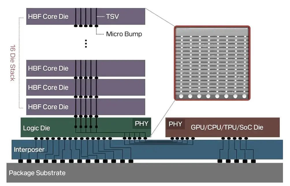
Next generation wafer bonding enables innovative types of memory This week, Samsung presented its vision for next-generation memory and storage solutions both for AI and general-purpose applications at the Future of Memory and Storage (FMS) 2026 conference. The company introduced zHBM, zNAND-O, and BV-NAND technologies at the event, and while they are aimed at very different applications, they share one common ingredient: they all rely on wafer bonding. Here's a breakdown of each type of technology that the company announced. * zHBM: Samsung's vision for custom HBM ultra-high-performance memory that will sit on top of logic dies. * zNAND-O: NAND memory that can be bonded atop a logic device to maximize bandwidth, reduce latency, and minimize power consumption. * BV-NAND (aka Samsung's 10 Generation V-NAND): Samsung's take on bonding NAND arrays atop all the circuitry needed to operate them. This is essentially next-generation 3D NAND technology that is used today by almost everyone, including Kioxia/Sandisk, SK Hynix, and YMTC (which was the first company to adopt such a method). zHBM: Placing HBM stack on top of logic Around the time we first heard about HBM4's 2,048-bit interface, we read a 'semi-official' report that SK hynix and its partners were considering vertical integration of HBM4 stacks on top of logic chips. To a large degree, companies were considering installing these memory stacks on top of their processors as they doubted that it would be possible and feasible to use interposers to connect HBM4 stacks to AI accelerators. Over time, it turned out that integration of memory on top of logic is complicated when it comes to cooling, power delivery, and developing interposers that can handle a 2,048-bit memory interface. Samsung's zHBM appears to be a continuation of that effort. Samsung's zHBM concept places HBM directly on top of an AI accelerator instead of on its perimeter, which greatly reduces the distance data must travel between compute and memory. The company says this architecture can increase bandwidth and power efficiency and projects that it can provide 8x the 'performance of HBM5', while its advanced wafer bonding is expected to enable over 10x higher memory density, 3x better energy efficiency, and more than 50% lower thermal resistance than HBM5. While Samsung's claims about the zHBM look incredibly impressive, they are vague. For example, when the company claims that a 'next-generation interface system incorporating zHBM' will deliver 'approximately eight times the performance of HBM5,' it never explicitly states whether this refers to memory bandwidth, actual application performance due to a combination of improvements over standard HBM, or something else. Had Samsung intended to compare raw bandwidth, it would likely have used more precise wording, such as '8x higher bandwidth.' Instead, the general term 'performance' may have many meanings. The same applies to references of improved power efficiency, higher memory density, and lower thermal resistance compared to HBM5, a standard that has not been fully defined or ratified. To make matters even more imprecise, Samsung mentions thermal resistance, which depends on implementation rather than the standard. Finally, Samsung didn't reveal which die stacking/bonding technology it will use for zHBM. In any case, Samsung says that zHBM will also support customer-specific designs and will enable custom IP to be integrated into the interconnect layer (which plays a role similar to the base die, though it is definitely not a base die per se) between the HBM stack and the AI processor, which essentially means that zHBM is not necessarily an industry-standard solution, so it might be implemented with additional perks. For now, Samsung hasn't disclosed any timeframes for when it plans to offer its zHBM solutions. The only clue is that it compares it to HBM5, which is likely to see the light of day sometime in the late 2020s or early 2030s. zNAND-O(on-device): Put storage close to compute Samsung also unveiled zNAND-O, a high-performance NAND memory currently in development that will enable putting four or eight stacks of NAND devices on top of logic dies. zNAND-O(n) device is based on the company's V-NAND platform (or rather, BV-NAND) and is meant to combine high storage density with improved I/O performance and low latency. Samsung claims that the tech is suitable for edge AI systems running real-time, data-intensive inference workloads, though, of course, there are many other applications that can benefit from high-performance on-package storage. Since the technology is in development, Samsung hasn't shared much information about it, even keeping the schematics of how it plans to put zNAND-O layers on top of a logic under wraps. We can speculate that since Samsung mentions 'improved I/O performance and low-latency,' it may be planning to exploit both the inherently parallel architecture of NAND memory with a high-performance interface, though we will not try to dive into details for the sake of not making the discussion too speculative. BV-NAND: Good old V-NAND gets a new treatment With BV-NAND, Samsung is essentially introducing a new brand name for its next-generation 3D NAND that bonds the NAND array on top of the I/O and logic wafer. This, in turn, produces the layer itself using high-performance logic process technologies and enables higher I/O speeds. Samsung formally announced its 400-layer-class V-NAND (aka 10 Generation V-NAND) some time ago, and even disclosed that its areal density would be 28 Gb/mm with a maximum I/O speed reaching 5600 MT/s. This likely stipulates the usage of a pinout that is different from the 3D NAND packages used today. While the areal density of Samsung's 10 Gen TLC V-NAND is slightly lower when compared to that of Kioxia/Sandisk's BiCS10 TLC NAND, its maximum I/O speed is significantly higher, which perhaps justifies the new branding. Considering the fact that Samsung rarely sells its memory to third parties and prefers to market client SSDs itself, a new brand for memory can be a sales driver, even if actual high-end drive performance is limited by a PCIe 5.0 x4 interface rather than by 3D NAND memory I/O. Then again, the performance of mid-range PCIe Gen5 SSDs that rely on a quad-channel NAND controller depends on 3D NAND I/O today, so marketing them under a new flash memory brand is a certain way to attract attention and then sell decent performance. Samsung's new brand strategy As the new name of the FMS tradeshow implies, the announcements touch upon very distinct industry needs. In the case of Samsung, we are talking about high-performance data center-grade AI accelerators; applications that need storage with latency that is lower than ~50 - 60 µs of modern high-end PCIe SSDs, though we will see how it compares to Z-NAND, and essentially a new generation of conventional 3D NAND with a new brand. Except for the 400-layer-class Samsung BV-NAND that is set to hit the market in the foreseeable future, the company's new tech, like zHBM and zNAND-O, is years away. Follow Tom's Hardware on Google News, or add us as a preferred source, to get our latest news, analysis, & reviews in your feeds.
[2]
Samsung Electronics launches next-generation AI memory technology
Aug 4 (Reuters) - Samsung Electronics (005930.KS), opens new tab introduced a new generation of artificial intelligence memory technology on Tuesday, seeking to reinforce its chipmaking lead in the booming AI market. The world's largest memory chip manufacturer chose this year's Future of Memory and Storage (FMS) conference in Santa Clara, California, to introduce its V10 Bonding V-NAND, or BV-NAND, prototype. The chip features more than 400 layers and a new wafer-bonding architecture to increase storage density and boost performance. As AI workloads have expanded beyond training large language models to the process of generating answers to user queries, demand for high-capacity NAND memory has increased. NAND flash memory is used to store data such as photos, videos and applications in devices including smartphones. The company said its BV-NAND technology increases memory density by about 58% from its previous V9 NAND while improving read, write and input/output performance to meet growing demand from AI systems requiring higher-capacity and more power-efficient storage. Samsung also showed concept models of what it described as the industry's first zHBM and zNAND-O architecture, outlining its vision for next-generation 3D memory that stacks memory cells vertically to pack in more data. Unlike conventional high-bandwidth memory, which is placed alongside AI processors, Samsung's zHBM stacks memory vertically above AI accelerators to reduce the distance data travels, increasing bandwidth while improving energy efficiency. Samsung said that its wafer-bonding technology could enable more than 10 times the memory density of conventional HBM5 memory while tripling energy efficiency and cutting thermal resistance by more than half. While some investors have voiced concern over long-term demand for memory chips once Chinese smartphone demand weakens, analysts have pointed to exceptionally strong AI demand. The robust nature of AI demand was emphasised by Samsung's disclosure last week that long-term agreements with customers could eventually account for 60% to 70% of its memory sales. Citi analysts said in a note last month that inventories across both DRAM and NAND supply chains remained well below historical levels despite concerns over softening end-market demand. Reporting by Heekyong Yang Editing by David Goodman Our Standards: The Thomson Reuters Trust Principles., opens new tab
[3]
Samsung announces next-gen 3D memory when all we want is reasonably priced DDR5 - Engadget
The new tech looks impressive, but most of it will be gobbled up by AI data centers. It used to be nice when Samsung announced its latest 3D memory or V-NAND storage, as we could all look forward to our PCs booting faster and files loading quicker. Now, the company has just announced its new next-gen memory and storage, and while the new tech looks impressive, it's depressing knowing that most of it will be gobbled up by AI data centers. At the Future of Memory and Storage (FMS) show in Santa Clara, Samsung unveiled the first concept models for zHBM, based on HBM memory used primarily in data centers, AI accelerators and a small number of high-end GPUs. zHBM is a new memory architecture that vertically stacks HBM directly above AI accelerators (rather than alongside them as before), helping boost performance up to eight times. It also uses next-generation wafer bonding tech, allowing over 10 times the memory density of current HBM5 tech while increasing energy efficiency threefold. Samsung also unveiled a new type of V-NAND memory used in SSDs, memory cards and other types of storage. Called V10 BV-NAND, it uses the company's new bonding V-NAND architecture to stack more than 400 layers of memory cells. This increases memory density by around 58 percent over the previous V9 generation, while boosting read, write and I/O performance. The company also introduced zNAND-O, a next-gen V-NAND solution combining "high space efficiency, improved I/O performance and low latency, aimed at edge AI environments. Finally, Samsung showcased LPDDR5X-PIM, the industry's first LPDDR memory with processing-in-memory technology, built to perform data processing within the memory itself to improve efficiency. Alongside SK Hynix, Samsung is one of two companies who control the majority of memory production. As Engadget's readers well know, both companies are failing to keep up with demand for memory created by the current AI bubble. That in turn is leading to insane prices for electronics of all kinds, ranging from gaming consoles to smartphones to laptops.
[4]
Samsung reveals next-gen memory with stacked HBM and 400-layer NAND
Serving tech enthusiasts for over 25 years. TechSpot means tech analysis and advice you can trust. In brief: Samsung is adding a new set of memory technologies to its AI strategy, using wafer bonding and 3D stacking to push bandwidth, density, and energy efficiency beyond what current high-bandwidth memory and NAND technologies can deliver. At the Future of Memory and Storage 2026 conference in Santa Clara, California, the company laid out a roadmap built around three main technologies: a new Bonding V-NAND architecture with more than 400 layers, a concept for vertically stacked high-bandwidth memory called zHBM, and a next-generation NAND approach called zNAND-O. These technologies target both large-scale AI training workloads in data centers and edge AI applications that require low latency and tight power controls. A key part of that strategy is zHBM, a new way of arranging high-bandwidth memory. In today's systems, HBM usually sits next to AI processors. zHBM instead stacks HBM directly on top of AI accelerators, placing the memory above the compute. This design shortens the physical distance data has to travel between the processor and memory, which is intended to increase bandwidth and improve power efficiency for large-scale AI training and inference. Samsung said a next-generation interface system using zHBM is expected to deliver about eight times the performance of HBM5. With wafer bonding, the company believes zHBM can achieve more than 10 times the memory density of HBM5 while improving energy efficiency threefold and cutting thermal resistance by more than half. The goal is to make high-capacity, high-bandwidth systems more stable and easier to cool. The zHBM concept also adds more flexibility to AI hardware design. It supports customer-specific layouts, allowing customized IP to sit in the layer between the memory stack and AI accelerator. That layer can be used to expand memory capacity or add logic tailored to particular AI workloads. zNAND-O is a high-performance NAND solution built on Samsung's V-NAND technology and aimed at edge AI. It is in development in four- and eight-layer versions. The company describes it as combining high space efficiency, improved input/output performance, and low latency to support real-time, data-intensive AI applications closer to where data is generated. That puts zNAND-O somewhere between traditional mass-storage NAND and memory products designed specifically for fast inference and local processing. The most concrete product announcement at the show was V10 BV-NAND, which Samsung presented as the industry's first Bonding V-NAND architecture. The device uses wafer bonding to stack memory cells and achieve more than 400 layers in a single chip. The higher layer count is designed to increase storage density and performance while reducing power consumption. Samsung said V10 BV-NAND boosts memory density by about 58% compared with its V9 generation. It also improves read, write, and input/output performance over V9, targeting high-performance, high-capacity NAND for future AI systems and applications.
[5]
Samsung Unveils Next-Gen 3D-Memory Vision at FMS 2026, Charting the Future of AI Infrastructure
Samsung introduces industry-first concept models of zHBM and zNAND-O, highlighting leadership in next-generation memory architecture for HPC and AI infrastructure 400-plus-layer V10 BV-NAND with wafer bonding technology revealed for the first time in industry AI memory roadmap spans next-generation solutions from DRAM to enterprise storage, including HBM4E, HBM5, LPDDR5X-PIM and PM1763 Samsung Electronics a global leader in advanced memory technology, today showcased its latest AI memory innovations at Future of Memory and Storage (FMS) 2026 in Santa Clara, California. With broad expertise spanning DRAM, NAND, enterprise storage and relevant advanced semiconductor technologies, Samsung presented its latest AI memory portfolio and technology roadmap, including a preview of its zHBM and zNAND-O concept models, the industry-first introduction of its V10 BV-NAND with 400-plus layers and a comprehensive range of solutions designed to advance future AI infrastructure. Samsung is also featuring its AI cloud server-inspired booth at FMS 2026, where approximately 30 memory and storage technologies are on display. At the opening keynote event, Samsung's Memory Business executives Jin-Yub Lee, Executive Vice President and Head of Flash Product & Technology and Kyungryun Kim, Vice President and Project Leader of the DRAM Design Team, delivered their address on next-generation 3D structures in future memory solutions. Titled "Driving the Wave of AI Revolution: 3D Innovations in Memory & Storage Architecture," the keynote presented Samsung's vision to maximize AI system performance and power efficiency while addressing the rapidly growing demands of high-performance computing (HPC) and AI infrastructure. The company also unveiled V10 BV-NAND, an architecture enabled by a new wafer bonding technology -- for the first time in the industry. Samsung's Vision for Next-Generation 3D Memory At FMS 2026, Samsung unveiled the industry's first concept models of zHBM and zNAND-O, presenting its vision for the next generation of 3D memory architectures. Designed for advanced AI computing, zHBM presents a new memory architecture that vertically stacks HBM directly above AI accelerators, moving beyond conventional designs in which HBM is positioned alongside the processor. By minimizing the distance that data travels between the AI processor and memory, zHBM is designed to deliver higher bandwidth and improved power efficiency, enabling the ultra-fast data processing required for large-scale AI training and inference. A next-generation interface system incorporating zHBM is expected to deliver approximately eight times the performance of HBM5. With next-generation wafer bonding technology, zHBM can achieve more than 10 times the memory density of HBM5 while enhancing energy efficiency threefold and reducing thermal resistance by more than half, maximizing the stability and power efficiency of high-capacity, high-bandwidth systems. zHBM also supports customer-specific designs, enabling customized IP to be integrated into the interlayer between the memory and AI accelerator to expand memory capacity and enhance accelerator performance. Building on close collaboration with customers, Samsung plans to further optimize the integration of AI processors and memory through zHBM to maximize AI system performance. The company also introduced zNAND-O, a next-generation high-performance NAND solution built on its V-NAND technology and in development in four- and eight-layer versions. By combining high space efficiency, improved I/O performance and low latency, zNAND-O is optimized for edge AI environments supporting real-time, data-intensive AI applications. Industry-First V10 BV-NAND Samsung unveiled V10 BV-NAND, featuring its new Bonding V-NAND architecture. The announcement comes 13 years after the company introduced the industry's first V-NAND technology at the 2013 Flash Memory Summit, marking another milestone in the company's NAND innovation. With more than 400 layers, V10 BV-NAND delivers higher performance and power efficiency while significantly increasing storage density. By applying wafer bonding technology to stack memory cells, Samsung has increased memory density by approximately 58% over the previous generation (V9). Beyond the increased layer count, V10 BV-NAND also improves read, write and I/O performance over the previous generation, supporting high-performance, high-capacity NAND for future AI systems and applications. AI Memory Roadmap from HBM to PIM and Enterprise Storage Samsung also presented its latest AI memory and storage portfolio -- including HBM4E, HBM5, LPDDR5X-PIM and PM1763 -- highlighting its roadmap for next-generation AI computing and data center infrastructure. Following the industry's first mass production of HBM4 using its 1c DRAM and 4-nanometer (nm) base die technologies in February, Samsung was the first to begin shipping HBM4E samples to global customers in May, reinforcing its leadership in next-generation HBM. Along with its HBM4E samples and HBM5 model, the company showcased its LPDDR5X-PIM, the industry's first LPDDR memory with processing-in-memory technology. The new solution is built to perform data processing within the memory itself to improve the efficiency of both data movement and power. The exhibition also featured Samsung's latest enterprise storage solutions -- including PM1763 and BM1773 -- designed to meet the growing storage demands of AI data centers. One-Stop Turnkey Solutions As the world's only integrated device manufacturer (IDM) with industry-leading capabilities spanning memory, foundry and advanced packaging, Samsung presented its end-to-end strategy for next-generation AI infrastructure, which provides customers with one-stop turnkey solutions supporting the evolving needs of the AI era. From product design through mass production, Samsung delivers integrated development and manufacturing services that help shorten development cycles while optimizing performance and power efficiency, enabling customers to quickly bring differentiated AI semiconductor solutions to market.
[6]
Samsung unveils zHBM memory chip concept for future AI servers
Samsung Electronics unveiled a new memory chip concept called zHBM for future AI servers, saying it could deliver about eight times the speed and more than 10 times the memory density of HBM5 chips. The company presented zHBM, short for Z-axis High Bandwidth Memory, at the Future of Memory and Storage 2026 expo in Santa Clara for use in advanced AI computing devices, including AI servers and data centers. Samsung said the gains would come from stacking HBM chips directly on top of an AI accelerator instead of placing them beside it on an interposer. The layout shortens the distance between processor and memory and is intended to improve data-transfer speeds. Samsung said zHBM could achieve 10 times the memory density of HBM5 through next-generation wafer-bonding technology. The company also said the design could provide three times better energy efficiency and 50% lower thermal resistance than conventional memory configurations. Samsung said zHBM could support customer-specific designs, allowing customized components to be integrated into the layer between the AI accelerator and the memory chip. The company said this could enable higher memory capacity and improve accelerator performance. Samsung did not announce a production timetable for zHBM. The concept is expected to follow HBM5, which the source material said could reach customers sometime in 2028, implying a commercial launch for zHBM after that year.
[7]
Samsung reveals zHBM: future RAM is stacked above AI accelerator, boasts 8x performance of HBM5 and 3x energy efficiency
Samsung has been showing off a future innovation for memory in the form of zHBM, among other revelations at the Future of Memory and Storage (FMS) conference. FMS 2026 is happening in Santa Clara, California, where, as VideoCardz spotted, Samsung introduced us to both zHBM and zNAND-O which are next-gen 3D memory architectures, albeit they are only at the concept stage right now. Given that, details are scarce, but as the 'z' suggests, this tech is about stacking vertically (on the Z-axis). In the case of zHBM, this is a new take on HBM where the memory is directly stacked above the AI accelerator (as opposed to being placed alongside the processor as is the case currently). This cuts down the distance that data has to travel between the AI processor and the memory, with zHBM offering a higher bandwidth and better power-efficiency. Samsung claims that: "A next-generation interface system incorporating zHBM is expected to deliver approximately eight times the performance of HBM5. With next-generation wafer bonding technology, zHBM can achieve more than 10 times the memory density of HBM5 while enhancing energy efficiency threefold and reducing thermal resistance by more than half, maximizing the stability and power efficiency of high-capacity, high-bandwidth systems." In short, Samsung is promising a major leap forward. As for zNAND-O, this is a take in a similar vein for NAND. It uses Samsung V-NAND tech stacked in four and eight-layer versions, which again offers better performance and lower latency. It's optimized for "edge AI environments supporting real-time, data-intensive AI applications". All of this is a long way out, though, with no release dates for what are clearly early working concepts. Of course, most people aren't so worried about the future of memory technology, but more about when they might be able to buy today's RAM at a price which doesn't feel like a massive rip-off. Still, it's an interesting glimpse into the future nonetheless, particularly given the performance claims being made here for zHBM.
[8]
Samsung Tackles the Memory & Storage Wall With 400+ Layer "Hybrid Bonded" V10 BV-NAND & zHBM That Stacks HBM Directly On Top of AI Chips
Samsung has introduced brand new memory and storage technologies at FMS 2026, such as V10 BV-NAND, zHBM, and zNAND-O. Next-Gen AI Accelerators Will Stack Massive Vertical HBM Stacks Directly On Top of Them With Samsung's zHBM Tech As AI and compute requirements continue to grow, the current swath of technologies is starting to see drawbacks, requiring manufacturers to invest in transformative concepts that are going to play a fundamental role in future AI infrastructure. At FMS 2026, Samsung displayed two brand new technologies that are currently in concept stage, but would become a major deal moving forward if brought to life and implemented on real silicon, such as AI accelerators. The main technology highlighted is the zHBM memory solution. According to the company, zHBM takes the existing HBM design and places it directly above the AI accelerator. Currently, HBM is featured next to the main AI accelerator compute die, but having it on top of the AI accelerator is going to save space and offer better gains when it comes to data transfer speeds. zHBM is expected to deliver higher bandwidth and improved power efficiency. The company claims that zHBM will deliver an 8x performance leap over a conventional HBM5 solution, and over 10x gain in memory density while offering 3x the energy efficiency & cutting down thermal resistance by more than half. Samsung has reasons for not going into specifics of the tech since it's still in an early concept phase, but they do state that zHBM will offer flexibility in terms of customer-specific designs. Samsung is already working with its customers to further optimize the integration of zHBM on next-generation AI accelerators. zNAND-O Takes Storage Beyond Convention The second technology that is being unveiled is called zNAND-O, which is a high-performance and next-gen NAND solution built on the foundation of Samsung's V-NAND. This will come in 4- and 8-layer configurations and will combine high space efficiency, improved I/O performance, and low latency. zNAND O is designed for edge AI applications, though it isn't stated if this is the multi-stacked V-NAND tech that will be ready around 2030. Taking NAND Beyond 400 Layers And lastly, we have Samsung's next-generation NAND solution called V10 BV-NAND. This is going to be Samsung's first V-NAND architecture with hybrid bonding & takes NAND beyond 400 layers. It is said that with BV-NAND, Samsung's V10 storage designs will offer higher performance and power efficiency while boosting storage density massively. The technology is straightforward, leveraging hybrid bonding to stack memory cells together instead of making a single cell with denser layers. Memory density sees a 58% boost versus V9 NAND, and also improves read, write, and IO performance versus prior generations. We should mention that Samsung is already planning for 1000+ layers with hybrid bonding approaches, and BV-NAND has officially kicked off this trend. In the coming years, we are going to see a rapid increase in storage capacity across Samsung's SSD and Storage portfolio, while its memory solutions see a rapid and innovative pace with technologies such as zHBM, HBM4E, HBM5, GDDR7, and beyond. Follow Wccftech on Google to get more of our news coverage in your feeds.
[9]
Samsung's new memory chip could make Nvidia's AI chips faster
Anyone who has bought a fast new laptop only to watch it freeze while a file loads knows the frustration. The processor is not the problem. It is waiting on memory that cannot feed it fast enough, and that same bottleneck now sits between AI companies and faster models. Samsung Electronics says it has an answer. On Tuesday, Aug. 4, at the Future of Memory and Storage conference in Santa Clara, the company unveiled zHBM, a new way of stacking memory chips directly on top of AI processors instead of beside them, according to a Samsung press release. The timing was pointed. Two of Samsung's biggest rivals used the same event to unveil a completely different fix for the same problem. Conventional high-bandwidth memory sits next to the AI chip on the same package, and data still has to travel sideways before reaching the processor. zHBM stacks memory vertically above the chip instead, cutting that distance. A next-generation interface built around the design is expected to deliver about eight times the performance of today's HBM5, Reuters reported. Samsung said the same architecture could pack in more than 10 times the memory density of HBM5 while cutting energy use by two-thirds and thermal resistance by more than half, according to the company. For chipmakers such as Nvidia, that matters because memory bandwidth, not raw processing power, has become the limiting factor in how fast a data center can train and run AI models. Samsung also introduced V10 BV-NAND, a storage chip built with a new wafer-bonding technique that packs more than 400 layers into a single piece of silicon, according to the company. That design lifts storage density by about 58% over Samsung's previous generation, the V9, while improving read and write speeds, Reuters reported. The bottleneck has moved from chips to memory AI workloads have expanded beyond training large language models into generating responses for millions of daily users, pushing NAND demand sharply higher. Samsung disclosed last week that long-term supply agreements could soon account for 60% to 70% of its total memory sales, a sign that customers are locking in chips years before they need them. That is the real subtext behind the Aug. 4 showcase. Samsung is not just demonstrating engineering. It is trying to convince Nvidia and every hyperscaler that its memory will not be the reason their systems fall behind. NurPhoto / Getty Images SK Hynix and Sandisk are betting on a different memory fix SK Hynix and Sandisk used the same conference to release the first open-standard specification for High Bandwidth Flash, a technology built through the Open Compute Project with backing from Google and Tenstorrent, according to a Sandisk press release. Instead of racing to make memory faster, HBF adds a new layer of NAND-based capacity between HBM and SSDs, letting AI models too large for HBM alone stay closer to the processor. The two strategies playing out at the same event capture how differently the top three memory makers are approaching the same shortage: * Vertical stacking directly above the AI chip is Samsung's proprietary bet, aimed at squeezing more bandwidth out of a shorter physical path between memory and processor. * An open standard called High Bandwidth Flash is SK Hynix and Sandisk's alternative, adding NAND-based capacity so that AI models too large for HBM can still run near the chip. * Gaining ground through existing DRAM production, not new architecture, is Micron's near-term approach, and it is working. Micron is closing the gap while supply runs dry Micron lifted its global DRAM market share to 25% in the second quarter of 2026, up from 22%, closing in on SK Hynix's 26%, while Samsung held the top spot at 39%, GuruFocus reported. Micron (MU) shares jumped nearly 6% on the news, one of several recent sharp swings in memory stocks as investors price in who benefits most from the shortage. Innovation cannot fix what capacity cannot supply None of this changes a more basic constraint. Samsung, SK Hynix, and Micron have already sold out their entire 2027 DRAM and HBM production capacity, with customers receiving only 60% to 70% of the volumes they originally requested, according to a Seeking Alpha report citing industry sources. New architecture does not add a single wafer of supply. It only decides who gets more value out of the wafers that already exist. That is the part other coverage of the Aug. 4 announcement has mostly missed. Samsung, SK Hynix, and Sandisk are not competing on speed anymore. They are competing to become the default design inside a market that will not grow until new fabs finish construction in 2027 and 2028. Whoever wins that bet locks in pricing power for years, not just a headline at a trade show. For Nvidia and the hyperscalers relying on these components, the message is clear. The AI race is no longer just about who designs the smartest processors, but who can secure the memory to actually run them. Investors should watch closely to see whose architecture becomes the industry standard, as that company will quietly dictate the pace of the AI boom through the end of the decade. The Arena Media Brands, LLC THESTREET is a registered trademark of TheStreet, Inc. This story was originally published August 6, 2026 at 11:03 PM.
[10]
Samsung demos next-gen AI memory solutions at FMS 2026
At the Future of Memory and Storage (FMS) 2026 conference in Santa Clara, California, Samsung Electronics presented its latest portfolio of artificial intelligence (AI) memory innovations and an updated technology roadmap. Featuring an AI cloud server-inspired exhibition showcasing approximately 30 memory and storage technologies, the company outlined its strategic response to the increasing bandwidth and power demands of high-performance computing (HPC) and AI infrastructure. 3D Architectural Innovations: zHBM and zNAND-O During the opening keynote titled "Driving the Wave of AI Revolution: 3D Innovations in Memory & Storage Architecture," Samsung executives Jin-Yub Lee, Executive Vice President and Head of Flash Product & Technology, and Kyungryun Kim, Vice President and Project Leader of the DRAM Design Team, outlined the company's vision for 3D memory structures. Samsung introduced concept models for two new 3D architectures tailored for AI workloads: * zHBM (Vertical Stacking): Moving away from conventional side-by-side placements, zHBM vertically stacks High Bandwidth Memory directly on top of AI accelerators. By using wafer bonding technology and reducing signal travel distance, the system aims to achieve up to eight times the performance and more than ten times the memory density of HBM5. The design also targets a threefold increase in energy efficiency and cuts thermal resistance by more than half. Additionally, zHBM supports custom interlayer intellectual property (IP) integration between the processor and memory. * zNAND-O (Edge AI Storage): Built on Samsung's V-NAND foundation, zNAND-O is in development in four- and eight-layer configurations. It focuses on high spatial efficiency, improved I/O speeds, and low latency to support real-time data processing in edge computing environments. Introduction of V10 BV-NAND Architecture Marking 13 years since the debut of its initial V-NAND technology, Samsung unveiled V10 BV-NAND, the industry's first memory based on a Bonding V-NAND architecture. Comprehensive AI Memory and Enterprise Storage Roadmap Samsung outlined updates across its broader product portfolio spanning DRAM, NAND, processing-in-memory (PIM), and enterprise drives: * High Bandwidth Memory (HBM): Following the mass production of HBM4 using 1c DRAM and a 4-nanometer (nm) base die in February, Samsung initiated customer shipments of HBM4E samples in May. The company also presented concept previews for HBM5. * Processing-In-Memory (PIM): Samsung showcased LPDDR5X-PIM, an mobile memory solution that executes data processing within the memory module itself to minimize data movement and decrease overall power consumption. * Enterprise Solid-State Drives (SSDs): Updated storage models, including the PM1763 and BM1773, were highlighted to address capacity and throughput requirements in high-density AI data centers. End-to-End Integrated Manufacturing Strategy Positioning itself as an Integrated Device Manufacturer (IDM) with operations covering memory design, foundry fabrication, and advanced packaging, Samsung highlighted its ability to provide turnkey development. By consolidating design through mass production within a single pipeline, the company aims to reduce time-to-market and streamline power and performance optimization for customized AI hardware configurations.
[11]
Samsung introduces zHBM to stack memory vertically on logic chip - The Korea Times
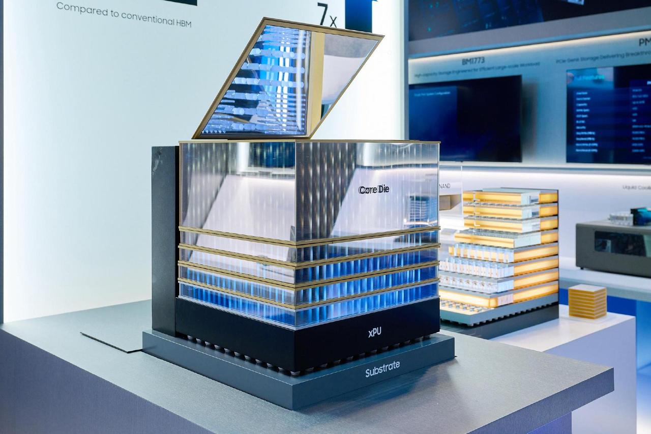
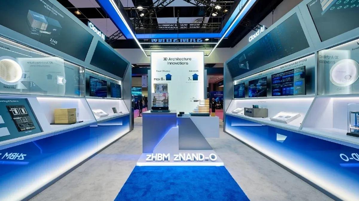
A mockup of Samsung Electronics' zHBM is displayed at its booth for the Future of Memory and Storage 2026 in California, Tuesday (local time). Courtesy of Samsung Electronics Samsung Electronics showcased its next-generation 3D memory architectures at the Future of Memory and Storage 2026 in California on Tuesday (local time), unveiling mockups of zHBM and zNAND-O. Samsung outlined its vision for 3D architectures for future memory solutions during a keynote speech by its memory business executives and exhibited mockups of the two new structures at its booth. ZHBM is an architecture aimed at improving the data processing speed of artificial intelligence (AI) accelerators by shortening the physical distance between logic processors -- central processing units, graphics processing units and others -- and high-bandwidth memory (HBM). While conventional HBM is placed beside logic chips, zHBM is stacked directly on top of the processor. By shortening the distance that data must travel, the new architecture delivers higher bandwidth and improved power efficiency. To support this architecture, Samsung applied hybrid copper bonding, multiwafer bonding and other advanced technologies, which together increase signal transfer speed while reducing thermal resistance. Samsung said an AI accelerator using zHBM can deliver up to eight times the performance of one equipped with HBM5. The shorter distance between the processor and memory also improves power efficiency by up to threefold compared with HBM5 and reduces thermal resistance by more than half. Given that major memory makers are currently mass-producing HBM4 and conducting sample tests of next-generation HBM4E, zHBM represents a longer-term architecture envisioned for memory solutions beyond the current HBM roadmap. ZHBM also supports customer-specific designs, enabling customized intellectual property blocks to be integrated into the interlayer between the memory and AI accelerator to expand memory capacity and enhance accelerator performance. The company also introduced zNAND-O, a next-generation high-performance NAND architecture built on its V-NAND technology and available in four- and eight-layer versions. By combining high space efficiency, improved performance and low latency, zNAND-O is optimized for edge AI environments supporting real-time, data-intensive AI applications. Also at the exhibition, the company unveiled V10 BV-NAND, featuring its new Bonding V-NAND architecture. With more than 400 layers, the new product delivers higher performance and power efficiency while significantly increasing storage density.
Share
Copy Link
Samsung unveiled three next-generation memory technologies at the Future of Memory and Storage 2026 conference. The company introduced zHBM, a vertically stacked high-bandwidth memory architecture, zNAND-O for edge AI applications, and V10 BV-NAND featuring over 400 layers. All three technologies leverage advanced wafer bonding to address the growing demands of AI data centers and infrastructure.
Samsung Electronics presented three next-generation memory technologies at the Future of Memory and Storage (FMS) 2026 conference in Santa Clara, California, marking a shift in how AI memory will be designed and deployed.
1
2
The world's largest memory chip manufacturer unveiled zHBM, zNAND-O, and V10 BV-NAND, all built on advanced wafer bonding technologies that promise to reshape AI infrastructure.5
This announcement comes as AI workloads expand beyond training large language models to the process of generating answers to user queries, driving demand for higher-capacity, more efficient memory solutions.2
Source: Samsung
Samsung's zHBM concept represents a fundamental change in memory architecture, placing HBM directly on top of AI accelerators instead of positioning it on the perimeter.
1
4
This vertical stacking approach shortens the physical distance data must travel between compute and memory, designed to increase bandwidth and improve power efficiency for large-scale AI training and inference workloads.5
Source: Korea Times
Samsung projects that a next-generation interface system incorporating zHBM will deliver approximately eight times the performance of HBM5.
2
5
The company's wafer bonding technology is expected to enable more than 10 times higher memory density compared to HBM5, while improving energy efficiency threefold and reducing thermal resistance by more than 50%.1
2
The technology also supports customer-specific designs, allowing customized IP to be integrated into the interlayer between the memory stack and AI accelerator to expand memory capacity and enhance accelerator performance.5
Samsung revealed V10 BV-NAND, the industry's first Bonding V-NAND architecture featuring more than 400 layers.
2
5
This announcement arrives 13 years after the company introduced the industry's first V-NAND technology at the 2013 Flash Memory Summit.5
The new wafer-bonding architecture stacks memory cells to achieve unprecedented storage density and boost performance.2
BV-NAND increases memory density by approximately 58% compared to Samsung's previous V9 NAND generation.
2
4
Beyond the increased layer count, V10 BV-NAND improves read, write, and input/output performance to meet growing demand from AI systems requiring higher-capacity and more power-efficient storage.2
4
This technology is essentially next-generation 3D NAND that bonds NAND arrays atop all the circuitry needed to operate them, a method already adopted by companies like Kioxia/SanDisk, SK Hynix, and YMTC.1
Related Stories
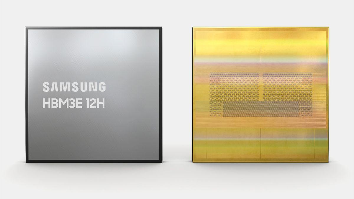
Samsung introduced zNAND-O, a next-generation high-performance NAND solution currently in development in four- and eight-layer versions.
4
5
Built on the company's V-NAND platform, zNAND-O is designed to enable putting multiple stacks of NAND devices on top of logic dies.1
Source: TweakTown
By combining high space efficiency, improved I/O performance, and low latency, zNAND-O is optimized for edge AI environments supporting real-time, data-intensive inference workloads.
2
5
The technology targets edge AI systems that require low latency and tight power controls, placing storage closer to compute for applications that process data near its source.4
Samsung's announcements come at a time when AI demand for memory chips remains exceptionally strong. The company disclosed last week that long-term agreements with customers could eventually account for 60% to 70% of its memory sales.
2
Citi analysts noted that inventories across both DRAM and NAND supply chains remained well below historical levels despite concerns over softening end-market demand.2
Alongside SK Hynix, Samsung controls the majority of memory production. Both companies are struggling to keep up with demand created by AI infrastructure expansion, leading to elevated prices for electronics ranging from gaming consoles to smartphones to laptops.
3
While Samsung's new technologies look impressive, most of the production capacity will likely be allocated to AI data centers rather than consumer applications.3
Samsung also presented its broader AI memory roadmap at FMS 2026, including HBM4E, HBM5, LPDDR5X-PIM, and PM1763 enterprise storage solutions.
5
The company began mass production of HBM4 using its 1c DRAM and 4-nanometer base die technologies in February and was first to ship HBM4E samples to global customers in May.5
Samsung hasn't disclosed specific timeframes for when zHBM will be available, though comparisons to HBM5 suggest commercialization in the late 2020s or early 2030s.1
Summarized by
Navi
[1]
[3]
1
Technology

2
Technology

3
Science and Research