SanDisk proposes stacking HBF NAND beneath GPUs to tackle memory bottlenecks in AI systems
2 Sources
[1]
SanDisk Proposes HBF NAND Stacks Beneath GPUs for AI Systems
SanDisk has outlined a new memory architecture concept called High-Bandwidth Flash (HBF), aimed at addressing one of the fastest-growing challenges in artificial intelligence computing: the need for significantly more memory capacity without relying entirely on increasingly scarce and expensive High Bandwidth Memory (HBM). The proposed HBF technology combines high-capacity NAND flash storage with advanced packaging techniques commonly associated with HBM. Instead of positioning storage devices away from the processor, SanDisk's design vertically stacks multiple NAND dies using through-silicon vias (TSVs), creating a compact storage structure that can be integrated much closer to the GPU. According to the company, one of the key advantages of HBF is capacity. Current HBM stacks typically provide between 32 GB and 64 GB of memory. HBF, by comparison, could scale to approximately 4 TB of storage capacity within a similar stacked architecture. This would allow future AI accelerators to keep substantially larger datasets physically closer to the compute engine. SanDisk's roadmap also includes a more ambitious implementation using a CMOS Bonded Array (CBA) design. In this configuration, HBF NAND would be positioned directly beneath the GPU package rather than beside it. The goal is to shorten data paths, improve transfer efficiency, and reduce latency compared to traditional storage arrangements. The company has already secured patent protection for aspects of the technology under U.S. Patent No. 12,430,274 B2. The architecture is not intended to replace HBM. Instead, both technologies would coexist within the same package and perform different functions. HBM would continue serving latency-sensitive workloads and high-priority real-time processing tasks, while HBF would act as a high-capacity storage layer for large AI models, training datasets, and less frequently accessed data. This tiered memory approach could offer multiple benefits. By reducing dependence on large quantities of HBM, future accelerator designs may be able to lower costs and partially alleviate current supply constraints affecting AI hardware manufacturers. It could also provide a practical way to increase available memory capacity without dramatically expanding package size. Despite its potential, HBF remains a long-term technology proposal rather than a near-term product. Several major technical challenges remain unresolved. Thermal management will be particularly demanding if NAND storage is placed directly beneath high-power AI processors. Manufacturing complexity, packaging costs, and integration of GPU, DRAM, and NAND components into a single package will also require significant development work. The proposal reflects a broader trend within the semiconductor industry as vendors search for new memory hierarchies capable of supporting increasingly demanding AI workloads. Whether HBF eventually reaches commercial deployment remains uncertain, but the concept demonstrates how future AI accelerators may combine multiple memory technologies to balance performance, capacity, power efficiency, and cost. FeatureDetails Technology NameHigh-Bandwidth Flash (HBF) DeveloperSanDisk Memory TypeStacked NAND Flash InterconnectThrough-Silicon Vias (TSVs) Maximum Projected CapacityUp to 4 TB per stack Companion MemoryHBM DRAM Package IntegrationCMOS Bonded Array (CBA) GPU PlacementNAND Positioned Beneath GPU Primary PurposeAI Training and Inference Workloads StatusPatent and Technology Roadmap Stage PatentUS 12,430,274 B2 Source: SanDisk / Wccftech, @seti_park , @jimmy_yoasobi
[2]
SanDisk Bets on Stacking NAND and Compute on One Chip as HBM Shortages Choke the AI Boom
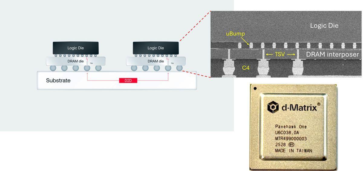
SanDisk is looking for more innovative solutions to address memory limitations, such as stacking NAND Flash within chips. Memory Limitations Push DRAM/NAND Maker To Get More Innovative, SanDisk Proposes The Stacking of NAND Flash Within Chips The rapid rise of AI & the proportional demand for compute has led to the exposure of bottlenecks, which are pushing DRAM and NAND manufacturers into going with the out-of-the-box approach. In the past, chipmakers called it a day by introducing new memory technologies, and DRAM was the primary component. But the rise in costs, development/yield drawbacks, & increased power have led to a focus on other viable solutions. HBM was developing at a steady pace, but that is rapidly becoming a bottleneck due to shortages. HBM has other drawbacks too, such as lower capacities, and while DRAM makers are pumping out faster speeds and more capacities each generation, they have so far been unable to keep up with demand. HBM also resides beside the primary chip, meaning there are inter-latency drawbacks. Then there's NAND, which offers more capacities at a cheaper cost, but it resides further away from the chip, and data transfer is slower. NAND has also not been able to achieve the same levels of speed as DRAM (HBM). Bridging The Best of DRAM & NAND Together To overcome this, NAND manufacturer SanDisk laid out its plans for its HBF (High-Bandwidth Flash) solution a while back. HBF is said to use a similar architectural hierarchy as HBM, which is to stack multiple layers of NAND Flash on top of each other. Each layer will be connected using multiple TSVs (Through Silicon Vias), which will fuse all NAND packages into a singular stack. While HBM offers 32-64 GB capacities per stack right now, HBF will scale up to 4 TB capacities. While this solves the capacity and speed concerns, the future demands for AI and HPC require something more. And that's where SanDisk's most recent patent, "US 12,430,274 B2," comes in. The patent explores the idea of 3D Stacking a NAND Flash tile using CBA (CMOS Bonded Array) underneath the main compute tile, which could be an AI accelerator or a GPU. The solution still uses HBM DRAM on the same interposer, but it serves a different purpose. It's like shooting down two birds with one stone; the HBM does the memory work that needs to be attended to immediately, while the NAND Flash on the Memory Tile is used for Read/Write ops, and for larger sets of data. The NAND Flash offers wider connections between the compute chip and the memory tile, which offers a reduction in speed, cost, and power. A processing core includes a multi-core processor integrated directly onto a high bandwidth, high-capacity non-volatile memory. The processor may for example be a large graphics processing unit (GPU) or artificial intelligence (AI) processor. The non-volatile memory may comprise a CBA (CMOS bonded to array) memory tile having a single large NAND memory tile coupled together with a CMOS logic circuit tile. The integrated processor and CBA memory tile may be affixed to an interposer. The processing core may further include stacks of high bandwidth memory (HBM) semiconductor dies affixed to the interposer around one or more sides of the processor and CBA memory tile. Now, while this future may give us a glimpse at future methodologies that overcome the memory bottlenecks, it should be noted that this is still a patent. A lot of things, such as power draw, the price to manufacturer such a chip (housing both NAND and DRAM on a single package), & more, need to be addressed before we see anything even close to this becoming a reality. The patent creates a real, examined moat around this processor-on-NAND architecture -- especially the wide-interface, through-tile routing that is hard to duplicate. Yet the product rolling toward standardization today follows the simpler, market-ready "beside" approach. The most interesting story is still unfolding: whether SanDisk eventually closes the gap between what it has protected and what it is shipping. The announcement is the headline; the patent is the deeper strategic map. News Sources: @seti_park , @jimmy_yoasobi Follow Wccftech on Google to get more of our news coverage in your feeds.
Share
Copy Link
SanDisk has unveiled High-Bandwidth Flash (HBF), a memory architecture that stacks NAND flash directly beneath AI processors using advanced packaging. The technology could deliver up to 4 TB of storage capacity per stack, addressing HBM shortages and capacity constraints. While still in the patent stage, HBF represents a shift toward tiered memory solutions for AI workloads.
SanDisk Unveils High-Bandwidth Flash to Address AI Memory Challenges
SanDisk has introduced a memory architecture concept called High-Bandwidth Flash (HBF), designed to tackle one of the most pressing challenges facing AI systems today: the need for dramatically increased memory capacity without relying solely on scarce and expensive High Bandwidth Memory. The proposed technology combines high-capacity stacked NAND flash with advanced packaging techniques, vertically stacking multiple NAND dies using through-silicon vias (TSVs) to create a compact storage structure integrated much closer to GPUs and AI accelerators
1
. This approach marks a significant departure from traditional storage arrangements where NAND resides further away from the processor, introducing inter-latency drawbacks that hamper performance2
.
Source: Wccftech
HBF NAND Offers Massive Capacity Gains Over HBM
One of the defining advantages of HBF lies in its capacity potential. Current HBM stacks typically provide between 32 GB and 64 GB of memory, while HBF could scale to approximately 4 TB of storage capacity within a similar stacked architecture
1
. This massive increase would allow future AI accelerators to keep substantially larger datasets physically closer to the compute engine, addressing a critical bottleneck as AI models continue to grow in size and complexity. The rapid rise of the AI boom has exposed these memory limitations, pushing DRAM and NAND manufacturers toward more innovative solutions beyond traditional approaches2
.CMOS Bonded Array Design Places NAND Directly Beneath Processors
SanDisk's roadmap includes an ambitious implementation using a CMOS Bonded Array (CBA) design, where HBF NAND would be positioned directly beneath the GPU package rather than beside it. This configuration aims to shorten data paths, improve transfer efficiency, and reduce latency compared to conventional storage arrangements
1
. The company has secured patent protection for aspects of this technology under U.S. Patent No. 12,430,274 B2, which explores integrating NAND flash with compute tiles in a single package2
. The patent describes a processing core with a multi-core processor integrated directly onto high-bandwidth, high-capacity non-volatile memory, creating wider connections between the compute chip and memory tile to reduce speed, cost, and power constraints.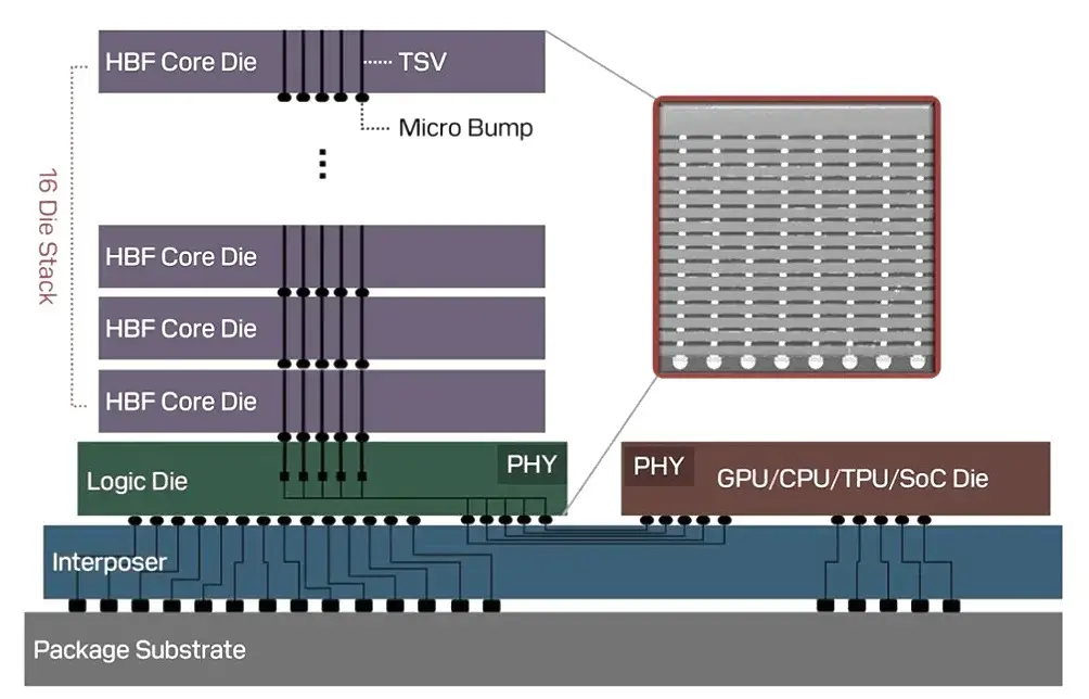
Source: Guru3D
Tiered Memory Architecture for AI Complements Rather Than Replaces HBM
The memory architecture for AI that SanDisk envisions does not seek to replace HBM entirely. Instead, both technologies would coexist within the same package, performing complementary functions. HBM would continue serving latency-sensitive workloads and high-priority real-time processing tasks, while HBF would act as a high-capacity storage layer for large AI models, training datasets, and less frequently accessed data
1
. This tiered approach bridges the best characteristics of DRAM and NAND together, with HBM handling immediate memory operations while NAND Flash on the memory tile manages read/write operations for larger data sets2
.Related Stories
Memory Solutions for AI Face HBM Shortages and Cost Pressures
By reducing dependence on large quantities of HBM, future accelerator designs may be able to lower costs and partially alleviate current supply constraints affecting AI hardware manufacturers. HBM shortages have become a significant bottleneck as demand for high-performance computing accelerates, and while DRAM makers are developing faster speeds and higher capacities each generation, they have struggled to keep pace with demand
2
. HBF could provide a practical way to increase available memory capacity without dramatically expanding package size, offering a path forward as AI workloads continue to intensify.Technical Hurdles Remain Before Commercial Deployment
Despite its potential, HBF remains a long-term technology proposal rather than a near-term product. Several major technical challenges must be resolved before commercial deployment becomes feasible. Thermal management will be particularly demanding if NAND storage is placed directly beneath high-power AI processors
1
. Manufacturing complexity, packaging costs, and the integration of GPU, DRAM, and NAND components into a single package will require significant development work. Questions around power draw and the price to manufacture such chips housing both NAND and DRAM on a single package need addressing before this becomes reality2
. The patent creates a strategic moat around this processor-on-NAND architecture, but whether SanDisk eventually closes the gap between what it has protected and what it ships remains to be seen. The proposal reflects a broader industry trend as vendors search for new memory hierarchies capable of supporting increasingly demanding AI workloads, signaling that future memory solutions will likely combine multiple technologies to balance performance, capacity, power efficiency, and cost.References
Summarized by
Navi
Related Stories
SK Hynix Develops High Bandwidth Storage Technology to Accelerate AI Performance in Mobile Devices
11 Nov 2025•Technology

SK hynix and SanDisk unite to standardize High Bandwidth Flash for AI inference servers
26 Feb 2026•Technology
Nvidia and SK Hynix develop AI SSD targeting 100 million IOPS to solve inference bottlenecks
17 Dec 2025•Technology
Recent Highlights
1
OpenAI releases GPT-5.6 models after government review, unveils ChatGPT Work to compete in AI agent race
Technology

2
Apple sues OpenAI over alleged trade secrets theft as 400+ former employees caught in scandal
Policy and Regulation

3
SK Hynix raises $26.5B in largest foreign US IPO as AI boom fuels memory chip demand
Business and Economy

Recent Highlights
Today's Top Stories


Don’t drown in AI news. We cut through the noise - filtering, ranking and summarizing the most important AI news, breakthroughs and research daily. Follow topics that matter to you and stay ahead.


