7 Sources
[1]
SK Hynix to invest $38 billion building new memory chip plants as demand soars
SK Hynix said on Friday it will invest 54 trillion Korean won ($38.1 billion) to build two new memory chip manufacturing plants, as demand for the components, which are key to AI, continues to grow. The South Korean tech giant announced a 35.2 trillion won investment in a fabrication plant, or fab, in Yongin called "Y2," with 19.1 trillion won earmarked for a facility in Cheongju called "M17." It comes amid a surge in memory prices driven by a shortage of supply and huge demand from companies building AI infrastructure like data centers and chip firms such as Nvidia, which require large amounts of high-bandwidth memory (HBM). The surge in memory prices has led to the biggest producers of the product -- SK Hynix, Samsung and Micron -- seeing a massive rally in their share prices as investors bet the supply imbalance will persist for some time. Yongin Y2 is the second of four fabs SK Hynix has planned in the Yongin Semiconductor Cluster. The company said it will serve as a production base for dynamic random access memory, or DRAM, which is in high demand. SK Hynix will break ground on construction in July 2027, with the opening of its first cleanroom in June 2029 to produce HBM and other next-generation DRAM products. A cleanroom is a controlled environment, which is key for chip manufacturing. SK Hynix said the Cheongju facility will produce NAND memory, a product for which "demand is surging rapidly," according to the company. The Cheongju M17 fab will break ground in February 2027 with the first cleanroom opening in December 2028. "In the AI era, technological competitiveness alone is not enough and the ability to supply the required volume at the exact moment customers need it is the ultimate competitive advantage," SK Hynix said in a press release. "We reached this investment decision after a thorough review of market demand." The investments form the next tranche of the company's "master plan," announced last year, which will see SK Hynix invest 600 trillion won in the Yongin Semiconductor Cluster and 100 trillion won to expand its Cheongju production base.
[2]
SK Hynix investing $38 billion in two new memory chip factories
The South Korean chipmaker approved 54 trillion won for fabs in Yongin and Cheongju, targeting cleanroom openings in 2028 and 2029 SK Hynix approved 54 trillion won ($38 billion) in investments on Friday, authorizing construction of two new fabrication plants on home soil -- one for DRAM and one for NAND flash -- as AI-driven appetite for memory chips shows no sign of slowing. The board earmarked 35.2 trillion won for the Yongin facility, known as Y2, and 19.1 trillion won for a second plant in Cheongju, designated M17, the company said. Y2 is set to begin construction in July 2027, with the facility's first cleanroom expected to come online in June 2029, focused on high-bandwidth memory and other advanced DRAM products. The Cheongju M17 fab will break ground in February 2027, with its first cleanroom set to open in December 2028. Both facilities fit within a broader strategic blueprint SK Hynix unveiled last year, which calls for 600 trillion won to be deployed across the Yongin Semiconductor Cluster and a further 100 trillion won directed toward expanding its Cheongju operations. Within the Yongin cluster, Y2 represents the second of four fabrication plants SK Hynix intends to build there. The company said it has accelerated its timeline to complete all four Yongin fabs by 2033, pulling forward the original 2045 target by 12 years. SK Hynix selected Cheongju for the NAND facility in part because the site already houses three existing fabs -- M11, M12, and M15 -- along with established power and water infrastructure, the company said. The Yongin cluster's Phase 1 power and water infrastructure, needed through Y2 operations, is 99% complete. "This investment is a decision made to seize opportunities in line with the market's growth speed," an SK Hynix official said in a statement. "By proactively securing production capabilities, we aim to establish ourselves as a key partner in AI infrastructure, contributing to the stability of the global AI semiconductor supply chain." The announcements follow a period of strong financial performance and rising demand. SK Hynix reported record quarterly operating profit of 60.54 trillion won in the second quarter, a 557% year-on-year increase, though the results fell short of analyst expectations. The company said cumulative first-half revenue crossed 100 trillion won for the first time in its history. SK Hynix CEO Kwak Noh-jung has warned that 2027 will bring the most severe memory supply shortage the industry has ever seen, with customer demand expected to outpace the company's production capacity beyond 2030. The company said it views current memory demand growth not as a temporary cycle but as a structural shift in which memory has become core AI infrastructure.
[3]
SK hynix approves $38B+ investment in two new memory fabs
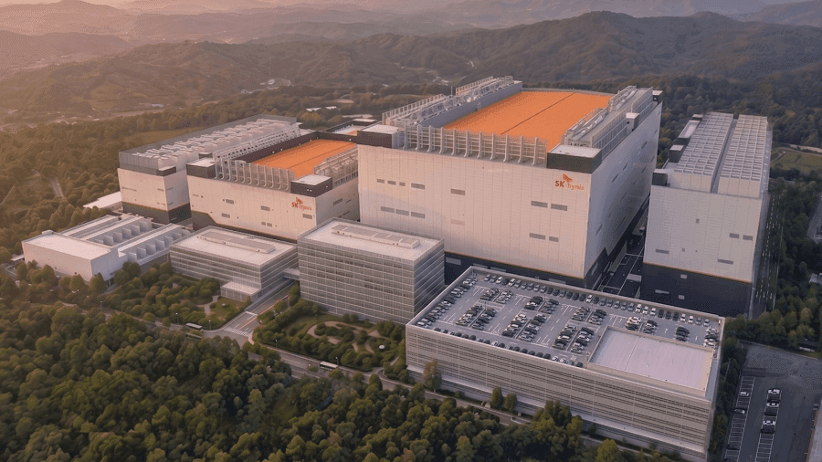
The board of SK hynix Inc., a major data center memory supplier, today approved the construction of two new fabs. The initiative will cost 54 trillion South Korean won, or about $38.3 billion. It's part of a broader $430 billion investment plan designed to expand SK hynix's manufacturing capacity. That initiative, in turn, is itself a component of a multibillion-dollar push by the South Korean government to grow the local chip sector. The latter project also includes SK hynix rival Samsung Electronics Co. SK hynix's newly announced construction initiative will see it build a $25 billion fab called Yongin Y2. It's the second of four chip factories that the company plans to build at the Yongin Semiconductor Cluster, a manufacturing campus about 20 miles south of Seoul. The first fab in the series is expected to open its doors next February. SK hynix plans to break ground on Yongin Y2 in July 2027. The facility's first cleanroom, a factory section that contains chipmaking equipment, is scheduled to come online in June 2029. The factory will have 279 acres of floor space once construction is complete. Yongin Y2 will be dedicated solely to DRAM manufacturing. SK hynix will use the fab to make, among other products, HBM memory. That's the high-speed RAM used by graphics cards to store artificial intelligence models and their data. SK hynix is the world's largest HBM producer. An HBM chip comprises multiple layers of RAM stacked atop one another, an arrangement that makes it possible to move data to and from the attached AI chip at high speed. SK hynix debuted its most advanced HBM device, a 12-layer chip, last September. It's based on a new version of the technology called HBM4. The standard provides more than twice the bandwidth of the memory that powers today's graphics cards. The second new fab that SK hynix plans to open will make NAND flash. It will be built on a campus that already hosts three of the company's chip factories. According to SK hynix, the existing power and water infrastructure on the site will speed up construction. The company expects to open the fab's first cleanroom in December 2028. Earlier this year, SK hynix and partner Sandisk introduced a new NAND flash technology called HBF. It stacks NAND flash circuits atop one another in a manner similar to HBM. According to the companies, the technology can match the performance of HBM while providing up to 16 times more capacity. Samsung, SK hynix's top rival in the memory market, is also developing vertical memory technologies. Today, NAND and HBM modules are placed next to the logic circuits of the host chip. On Wednesday, Samsung debuted two new technologies that make it possible to stack NAND and HBM memory directly atop logic circuits. That arrangement shortens the distance between components, which enables data to travel faster between them. The result is an increase in processing speeds. Samsung estimates that its stackable HBM technology will be eight times faster than HBM5, an upcoming version of HBM set to launch towards the end of the decade. The company also expects a tenfold increase in memory density, a measure of a RAM chip's capacity. Samsung will give customers the option to further optimize the technology by adding in custom interconnect components.
[4]
Global Market: SK Hynix approves $38.3 billion investment plan through 2031 to expand AI chip production
SK Hynix approved investments of 54.3 trillion won through 2031 to expand semiconductor production, targeting rising AI-driven demand. Funds will support new DRAM facilities in Yongin and NAND flash capacity in Cheongju. The company also plans additional shareholder return measures, with details expected during the third quarter, strengthening growth prospects. South Korean memory chipmaker SK Hynix has approved investments worth about 54.3 trillion won ($38.3 billion) through 2031 to expand its semiconductor manufacturing capacity, as the company ramps up production of advanced memory chips to meet growing demand driven by artificial intelligence (AI), according to Reuters. The company said its board has approved 35.2 trillion won for the second phase of construction at its semiconductor fabrication complex in Yongin and 19.1 trillion won for the M17 chip plant in Cheongju. US MarketsPowered By As on 07 Aug 2026, 01:30 AM IST S&P 500 Top Gainers Paycom Software215.97(23.55%) Motorola Solutions474.07(8.20%) Parker Hannifin1,070(7.31%) Leidos Holdings135.26(6.63%) Gainers" S&P 500 Top Losers AppLovin335.67(-19.66%) Datadog229.29(-19.03%) EPAM Systems93.07(-15.29%) Axon Enterprise522.46(-14.28%) Losers" The investment approval follows SK Hynix's announcement in June that it planned to invest 600 trillion won in the Yongin semiconductor cluster and 100 trillion won to expand production facilities in Cheongju. A Reuters report stated that the company had indicated at the time that detailed investment schedules would be released after receiving board approval. Yongin to Become Key DRAM Manufacturing Hub According to the company, the Y2 fabrication plant in Yongin will be the second of four planned chip fabrication facilities within the semiconductor cluster. The plant will primarily manufacture dynamic random access memory (DRAM) chips, which play a crucial role in servers supporting AI workloads. Construction of the Y2 facility is expected to begin in July 2027, while its first cleanroom is scheduled to become operational in June 2029. The facility will manufacture high-bandwidth memory (HBM) and other next-generation DRAM products, strengthening SK Hynix's position in the rapidly expanding AI memory market. The company also said development of the first-phase Yongin fabrication plant remains on schedule, with its first cleanroom expected to open in February 2027. Cheongju Expansion to Boost NAND Flash Output Separately, SK Hynix announced that construction of the M17 fabrication plant in Cheongju is scheduled to begin in February 2027. The facility will produce NAND flash memory, which is widely used for data storage across devices including personal computers, smartphones and AI servers. The first cleanroom at the M17 plant is expected to become operational in December 2028, the report stated. The Cheongju expansion is aimed at strengthening the company's production capacity across both DRAM and NAND memory segments as demand for advanced semiconductor components continues to rise. Shareholder Return Measures Under Review In a separate regulatory filing, SK Hynix said it is reviewing additional shareholder return initiatives aimed at enhancing shareholder value. According to Reuters, the company expects to finalize and announce the details of those measures during the third quarter, providing investors with further clarity on its capital allocation strategy.
[5]
What's Going On With SK hynix Stock Friday? - SK hynix (NASDAQ:SKHY)
SK Hynix Says AI Demand Is Structural -- Backs Claim With $39 Billion Investment The investment includes 35.2 trillion won for the Yongin "Y2" fabrication plant, which will focus on DRAM production, and 19.1 trillion won for the Cheongju "M17" plant, which will manufacture NAND flash memory. The company said the decision is part of its previously announced mid-to-long-term investment strategy. SK hynix plans to begin construction of the Yongin Y2 facility in July 2027, with its first cleanroom scheduled to open in June 2029. The fab will produce high-bandwidth memory (HBM) and other next-generation DRAM products. The Cheongju M17 facility is expected to break ground in February 2027 and open its first cleanroom in December 2028. AI Demand Drives Long-Term Investment The company cited forecasts from market research firm Omdia projecting both DRAM and NAND demand to grow at a 19% compound annual growth rate through 2030. SK hynix said it views the increase as a structural shift driven by AI rather than a temporary market cycle. Yongin Cluster And NAND Strategy The Yongin Semiconductor Cluster is designed to house four fabrication plants. SK hynix said the Y2 project supports its goal of completing the cluster by 2033, 12 years earlier than originally planned. For NAND, the company said demand for enterprise solid-state drives is accelerating alongside AI adoption, including increased use of key-value cache storage for AI inference workloads. It selected Cheongju for the new fab because existing infrastructure allows for a faster construction timeline. Production Ramp And Supply Chain Focus SK hynix said it will expand production capacity in line with customer demand by building the fabs on schedule while installing cleanrooms and manufacturing equipment in phases to maximize capital efficiency. An SK hynix official said the investment is intended to position the company as a key AI infrastructure partner while supporting the stability of the global AI semiconductor supply chain. SKHY Price Action: SK hynix shares were trading lower by 2.95% at $139.30 at the time of publication on Friday, according to Benzinga Pro data. Image via Shutterstock Market News and Data brought to you by Benzinga APIs To add Benzinga News as your preferred source on Google, click here.
[6]
Sk hynix to invest $38.3 bil. in Yongin's Y2 fab, Cheongju's M17 fab - The Korea Times
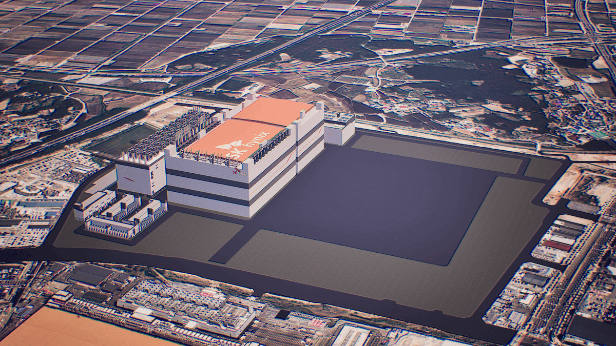
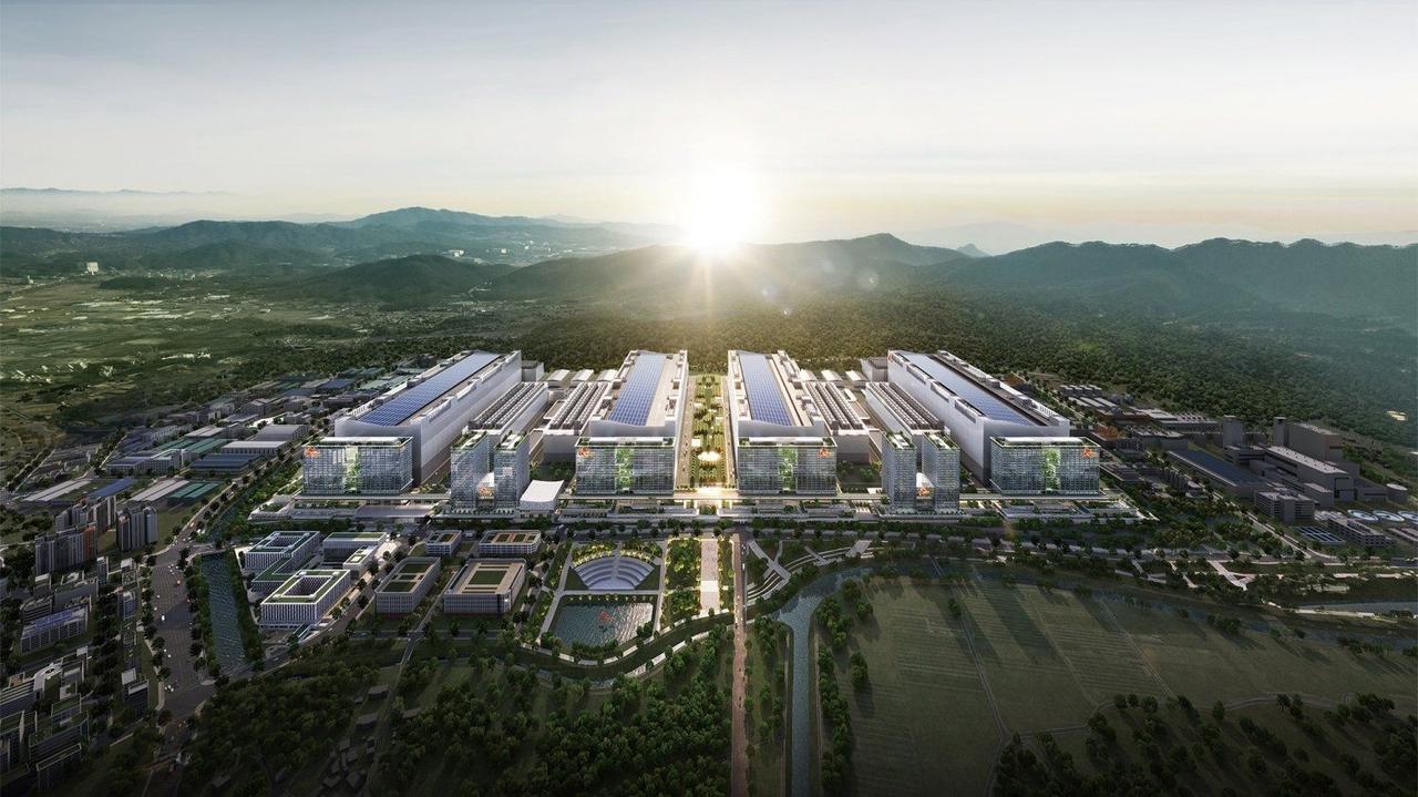
An artist's rendering of Yongin semiconductor cluster / Courtesy of SK hynix SK hynix Inc. said Friday it will invest a combined 54.3 trillion won ($38.3 billion) to build new semiconductor fabrication plants in response to rapidly growing demand for artificial intelligence (AI) memory chips. The investment plan, approved at a board meeting, includes 35.2 trillion won for the construction of the Y2 fab in Yongin, just south of Seoul, and 19.1 trillion won for the M17 fab in the central city of Cheongju, the world's second-largest maker of memory chips said in a regulatory filing. The decision marks the execution of SK hynix's mid- to long-term investment strategy and aligns with the government's "tripolar mega project" initiative, unveiled last month by President Lee Jae Myung to strengthen advanced technologies nationwide and position South Korea as a global industrial powerhouse in the AI era. Under its long-term investment plan, SK hynix has pledged to invest 600 trillion won in the Yongin semiconductor cluster and 100 trillion won to expand its production base in Cheongju. "In the AI era, technological competitiveness alone is not enough and the ability to supply the required volume at the exact moment customers need it is the ultimate competitive advantage," SK hynix said in a press release. Y2 will be the second of four fabs planned for the Yongin semiconductor cluster. Construction of the Y2 fab is scheduled to begin in July next year, with the first cleanroom expected to open in June 2029 for the production of high-bandwidth memory (HBM) and other next-generation dynamic random-access memory (DRAM) products. Construction of Y1 is also progressing as planned, with its first cleanroom scheduled to open in February next year. SK hynix previously announced plans to complete the Yongin semiconductor cluster by 2033, bringing forward the original completion target of 2045 by 12 years. The Y2 project represents the second phase of that accelerated expansion, with investment continuing through October 2031. The company selected Cheongju as the site for its new NAND flash memory fab because it offers the shortest construction timeline. The Cheongju campus already houses the M11, M12 and M15 fabs, allowing efficient integration with existing production facilities and infrastructure, including power and water supplies, SK hynix said.
[7]
SK hynix Inc. Invests In New Fabs In Yongin And Cheongju To Expand Production Base
SK hynix Inc. has decided to build new fabs in Yongin and Cheongju to respond to the continuously growing demand for memory in the AI era. The company approved a total investment of approximately KRW 54 trillion, KRW 35,200,000 million in Yongin "Y2" fab and KRW 19,100,000 million in the Cheongju "M17" fab, in a board meeting. Under its master plan to invest KRW 600,000,000 million in the Yongin Semiconductor Cluster and KRW 100,000,000 million to expand its Cheongju production base, SK hynix is currently constructing its first fab in Yongin (Y1). With this latest decision, the company is embarking on the construction of subsequent fabs in both Yongin and Cheongju. Yongin Y2 is the second of four fabs planned sequentially for the Yongin Semiconductor Cluster. It will serve as a DRAM production base spanning a total floor area of 341,000 pyeong (approximately 1,130,000m2). Construction is scheduled to break ground in July next year, targeting the opening of its first cleanroom in June 2029 to produce high-bandwidth memory (HBM) and other next-generation DRAM products. Construction on Y1 is progressing smoothly toward its initial cleanroom opening target of February next year. SK hynix previously set a goal to advance the completion date of the Yongin Semiconductor Cluster by 12 years?from the originally planned 2045 to 2033?to finish constructing all four fabs. The Y2 construction serves as the second phase supporting this accelerated timeline and the investment spans to October 2031 sequentially. The investment amount includes construction costs for "Business Support Building" with administrative and welfare facilities for Y2 personnel, an "Integrated R&D Center" to consolidate product development testing, analysis, and experiments, as well as auxiliary infrastructure. For the Yongin Semiconductor Cluster?sprawling over approximately 1,260,000 pyeong (approximately 4,160,000m2) in Wonsam-myeon, Cheoin-gu, Yongin-si, Gyeonggi-do?Phase 1 power and water infrastructure required up through Y2 operation is nearing completion, currently at a 99% progress rate. As fab construction and infrastructure setup have been carried out concurrently, the company plans to proceed with the Y2 construction according to schedule. SK hynix selected Cheongju as its new NAND fab base because it offers the fastest fab construction timeline. The Cheongju Campus already houses the M11, M12, and M15 fabs, enabling efficient production linked to existing operations on sites equipped with substantial pre-established power and water infrastructure. Cheongju M17 will be built across a total area of 206,000 pyeong (approximately 680,000m2), breaking ground in February next year with plans to open its first cleanroom in December 2028. The investment period runs through April 2031 according to the master plan. SK hynix plans to proactively secure production infrastructure based on mid-to-long-term demand discussed with customers, while expanding actual production capacity in alignment with the timing of customer needs. Fabs will be constructed according to the master schedule, whereas cleanroom expansions and equipment installation will take place sequentially in line with demand trends to maximize capital efficiency. The company expects this investment to secure future growth foundations while strengthening the competitiveness of the domestic semiconductor ecosystem and boosting local economies. The large-scale simultaneous investments in Yongin and Cheongju are anticipated to expand joint growth opportunities for supply chain partners, generate employment, and revitalize local commercial districts, thereby contributing to the sustainable growth of the national economy.
Share
Copy Link
SK Hynix approved 54 trillion won ($38.1 billion) to build two new fabrication plants in South Korea, targeting AI-driven memory chip demand. The Yongin Y2 facility will produce high-bandwidth memory and DRAM, while the Cheongju M17 plant will manufacture NAND flash. Construction begins in 2027, with cleanrooms opening between 2028-2029.
SK Hynix approved investments totaling 54 trillion won ($38.1 billion) on Friday to construct two new memory chip manufacturing plants, responding to what the company describes as a structural shift in AI-driven demand rather than a temporary market cycle
1
. The South Korean chipmaker allocated 35.2 trillion won for the Yongin Y2 fab and 19.1 trillion won for the Cheongju M17 facility, both designed to produce components critical to AI infrastructure2
. This investment represents the next phase of SK Hynix's master plan announced last year, which commits 600 trillion won to the Yongin Semiconductor Cluster and 100 trillion won to expand its Cheongju production base1
.
Source: Benzinga
The decision comes as memory prices surge due to supply shortages and massive demand from companies building AI infrastructure like data centers and chip firms such as Nvidia, which require substantial amounts of high-bandwidth memory (HBM)
1
. SK Hynix CEO Kwak Noh-jung has warned that 2027 will bring the most severe memory supply shortage the industry has ever seen, with customer demand expected to outpace production capacity beyond 20302
.The Yongin Y2 facility represents the second of four fabrication plants SK Hynix intends to build within the Yongin Semiconductor Cluster, located about 20 miles south of Seoul
3
. Construction will break ground in July 2027, with the first cleanroom scheduled to open in June 20291
. The facility will span 279 acres and focus exclusively on DRAM production, including high-bandwidth memory and other next-generation DRAM products3
.
Source: SiliconANGLE
SK Hynix currently holds the position as the world's largest HBM producer
3
. The company debuted its most advanced HBM device, a 12-layer chip based on HBM4 technology, last September, providing more than twice the bandwidth of memory powering current graphics cards3
. The company has accelerated its timeline to complete all four Yongin fabs by 2033, pulling forward the original 2045 target by 12 years2
. Phase 1 power and water infrastructure needed through Y2 operations is 99% complete2
.The Cheongju M17 fab will manufacture NAND flash memory, a product for which SK Hynix reports demand is "surging rapidly"
1
. Construction begins in February 2027, with the first cleanroom expected to become operational in December 20284
. SK Hynix selected Cheongju for the NAND facility because the site already houses three existing fabs—M11, M12, and M15—along with established power and water infrastructure that will accelerate construction2
.NAND flash memory is widely used for data storage across devices including personal computers, smartphones, and AI servers
4
. The company noted that demand for enterprise solid-state drives is accelerating alongside AI adoption, including increased use of key-value cache storage for AI inference workloads5
. Earlier this year, SK Hynix and partner Sandisk introduced HBF technology, which stacks NAND flash circuits in a manner similar to HBM and can match HBM performance while providing up to 16 times more capacity3
.Related Stories
SK Hynix cited forecasts from market research firm Omdia projecting both DRAM and NAND demand to grow at a 19% compound annual growth rate through 2030
5
. The company views this increase as a structural shift driven by AI rather than a temporary market cycle, with memory having become core AI infrastructure2
. An SK Hynix official stated, "This investment is a decision made to seize opportunities in line with the market's growth speed. By proactively securing production capabilities, we aim to establish ourselves as a key partner in AI infrastructure, contributing to the stability of the global AI semiconductor supply chain"2
.The company reported record quarterly operating profit of 60.54 trillion won in the second quarter, representing a 557% year-on-year increase, though results fell short of analyst expectations
2
. Cumulative first-half revenue crossed 100 trillion won for the first time in SK Hynix's history2
. The surge in memory prices has led major producers—SK Hynix, Samsung, and Micron—to experience significant rallies in share prices as investors anticipate the supply imbalance will persist1
.Samsung, SK Hynix's top rival in the memory market, is also developing vertical memory technologies
3
. Samsung recently debuted two technologies that enable stacking NAND and HBM memory directly atop logic circuits, shortening the distance between components and increasing processing speeds3
. Samsung estimates its stackable HBM technology will be eight times faster than HBM5, an upcoming version set to launch toward the end of the decade, with a tenfold increase in memory density3
.SK Hynix's investment is part of a broader multibillion-dollar push by the South Korean government to grow the local chip sector, which also includes Samsung Electronics
3
. The company stated, "In the AI era, technological competitiveness alone is not enough and the ability to supply the required volume at the exact moment customers need it is the ultimate competitive advantage"1
. SK Hynix also announced it is reviewing additional shareholder return initiatives aimed at enhancing shareholder value, with details expected during the third quarter4
.Summarized by
Navi
[3]
02 Jul 2026•Business and Economy

18 Nov 2025•Business and Economy

13 Jan 2026•Business and Economy

1
Technology

2
Technology

3
Science and Research